Embedded Flash memory (FLASH) RM0351
132/1830 DocID024597 Rev 5
3.7.12 Flash Bank 1 WRP area B address register (FLASH_WRP1BR)
Address offset: 0x30
Reset value: 0x00XX 00XX. Register bits are loaded with values from Flash memory at
OBL.
Access: no wait state when no Flash memory operation is on going, word, half-word and
byte access
3.7.13 Flash Bank 2 PCROP Start address register (FLASH_PCROP2SR)
Address offset: 0x44
Reset value: 0xFFFF XXXX
Access: no wait state when no Flash memory operation is on going, word, half-word access.
Bits 23:16 WRP1A_END: Bank 1 WRP first area “A” end offset
WRP1A_END contains the last page of the Bank 1 WRP first area.
Bits 15:8 Reserved, must be kept cleared
Bits 7:0 WRP1A_STRT: Bank 1 WRP first area “A” start offset
WRP1A_STRT contains the first page of the Bank 1 WRP first area.
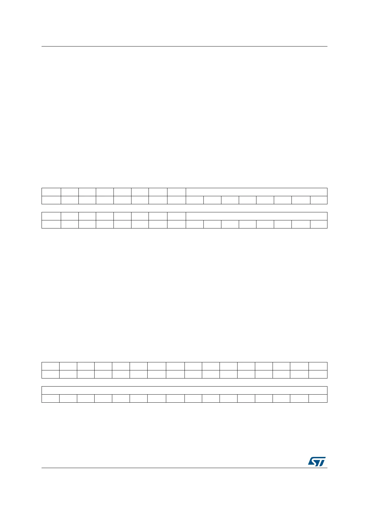
31 30 29 28 27 26 25 24 23 22 21 20 19 18 17 16
Res. Res. Res. Res. Res. Res. Res. Res. WRP1B_END[7:0]
rw rw rw rw rw rw rw rw
15 14 13 12 11 10 9 8 7 6 5 4 3 2 1 0
Res. Res. Res. Res. Res. Res. Res. Res. WRP1B_STRT[7:0]
rw rw rw rw rw rw rw rw
Bits 31:24 Reserved, must be kept cleared
Bits 23:16 WRP1B_END: Bank 1 WRP second area “B” end offset
WRP1B_END contains the last page of the Bank 1 WRP second area.
Bits 15:8 Reserved, must be kept cleared
Bits 7:0 WRP1B_STRT: Bank 1 WRP second area “B” start offset
WRP1B_STRT contains the first page of the Bank 1 WRP second area.
31 30 29 28 27 26 25 24 23 22 21 20 19 18 17 16
Res. Res. Res. Res. Res. Res. Res. Res. Res. Res. Res. Res. Res. Res. Res. Res.
1514131211109 8 765432 1 0
PCROP2_STRT[15:0]
rw rw rw rw rw rw rw rw rw rw rw rw rw rw rw rw
Bits 31:16 Reserved, must be kept cleared
Bits 15:0 PCROP2_STRT: Bank 2 PCROP area start offset
PCROP2_STRT contains the first double-word of the Bank 2 PCROP area.
 Loading...


