DocID024597 Rev 5 1625/1830
RM0351 USB on-the-go full-speed (OTG_FS)
1774
47.4 USB OTG functional description
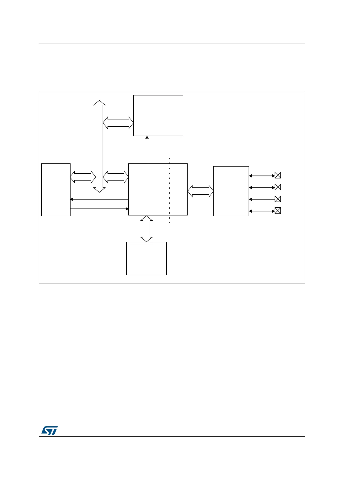
47.4.1 USB OTG block diagram
Figure 517. OTG full-speed block diagram
47.4.2 OTG core
The USB OTG receives the 48 MHz clock from the reset and clock controller (RCC), via an
external quartz. The USB clock is used for driving the 48 MHz domain at full-speed
(12 Mbit/s) and must be enabled prior to configuring the OTG core.
The CPU reads and writes from/to the OTG core registers through the AHB peripheral bus.
It is informed of USB events through the single USB OTG interrupt line described in
Section 47.13: OTG_FS interrupts.
The CPU submits data over the USB by writing 32-bit words to dedicated OTG locations
(push registers). The data are then automatically stored into Tx-data FIFOs configured
within the USB data RAM. There is one Tx FIFO push register for each in-endpoint
(peripheral mode) or out-channel (host mode).
The CPU receives the data from the USB by reading 32-bit words from dedicated OTG
addresses (pop registers). The data are then automatically retrieved from a shared Rx FIFO
configured within the 1.25-Kbyte USB data RAM. There is one Rx FIFO pop register for
each out-endpoint or in-channel.
$0
$-
)$
6
"53
/4'
&3
0(9
53"
/4'&3
#ORE
54-)&3
+BYTES
53"DATA
&)&/S
!("0ERIPHERAL
0OWER
#LOCK
#42,
53")NTERRUPT
53"SUSPEND
53"#LOCKAT-(Z
#ORTEXCORE
3YSTEMCLOCK
DOMAIN
53"CLOCK
DOMAIN
5NIVERSALSERIALBUS
2!-BUS
-36
 Loading...


