Liquid crystal display controller (LCD) RM0351
770/1830 DocID024597 Rev 5
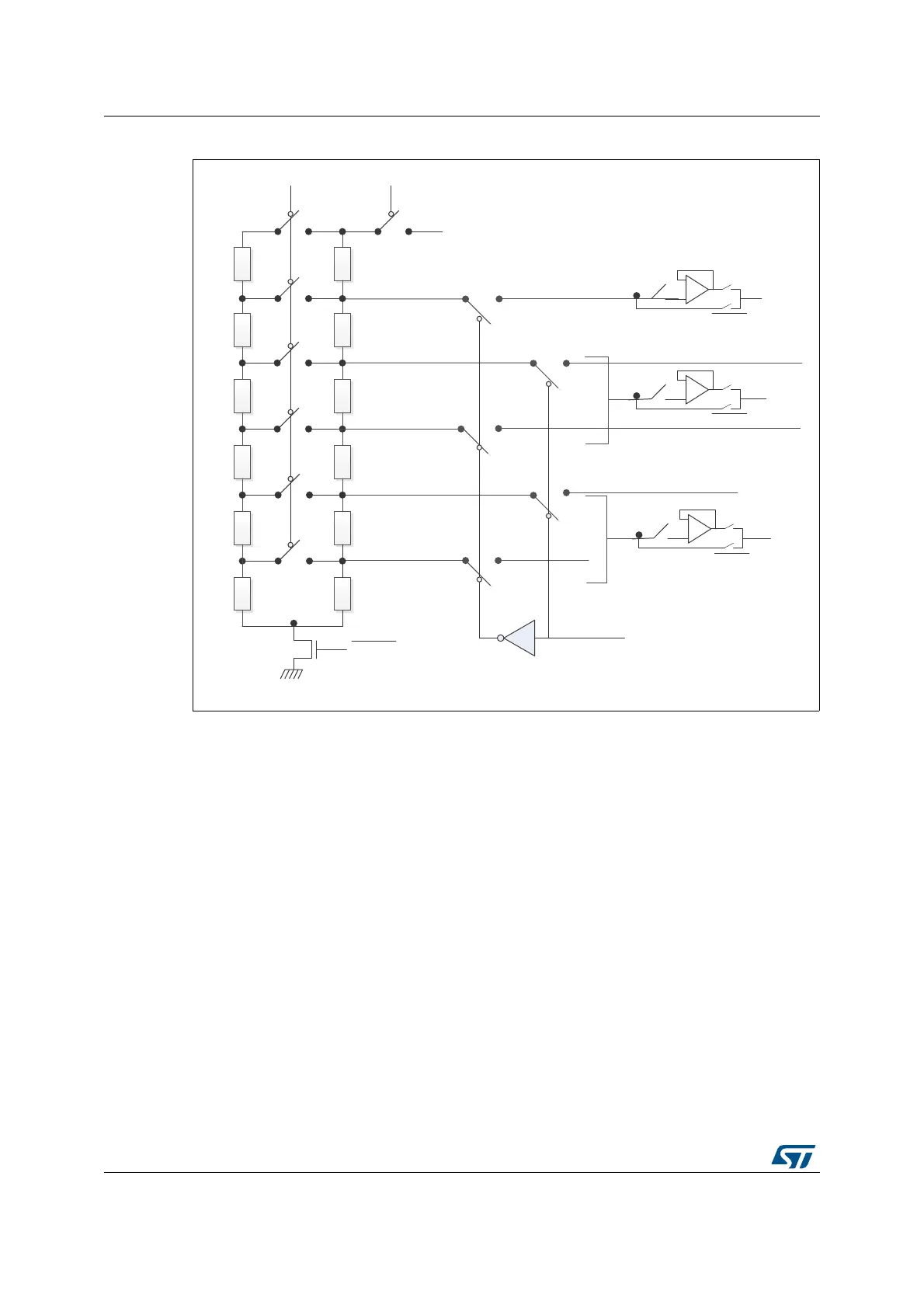
Figure 179. LCD voltage control
1. R
LN
and R
HN
are the low value resistance network and the high value resistance network, respectively.
The R
LN
divider can be always switched on using the HD bit in the LCD_FCR configuration
register (see Section 25.6.2).
The HD switch follows the rules described below:
• If the HD bit and the PON[2:0] bits in the LCD_FCR register are reset, then HD switch
is open.
• If the HD bit in the LCD_FCR register is reset and the PON[2:0] bits in the LCD_FCR
are different from 00 then, the HD switch is closed during the number of pulses defined
in the PON[2:0] bits.
• If HD bit in the LCD_FCR register is 1 then HD switch is always closed.
Buffered mode
When voltage output buffers are enabled by setting BUFEN bit in the LCD_CR register, LCD
driving capability is improved as buffers prevent the LCD capacitive loads from loading the
resistor bridge unacceptably and interfering with its voltage generation. As a result we
obtain more stable intermediate voltage levels thus improving RMS voltage applied to the
LCD pixels.
069
[9
/&'
[9
/&'
[9
/&'
[9
/&'
[9
/&'
9
/&'5DLO
%,$6>@
5
+
5
+
5
+
5
+
5
+
5
+
9
/&'
5
/
5
/
5
/
+'
(1
67$7,&
9
66
5
/
5
/
5
/
%8)(1
%8)(1
%8)(1
9
/&'5DLO
%8)(1
%8)(1
%8)(1
9
/&'5DLO
%8)(1
%8)(1
%8)(1
 Loading...


