Digital camera interface (DCMI) RM0351
650/1830 DocID024597 Rev 5
The camera interface can capture 8-bit, 10-bit, 12-bit or 14-bit data depending on the
EDM[1:0] bits in the DCMI_CR register. If less than 14 bits are used, the unused input pins
must be connected to ground.
shows the DCMI pins.
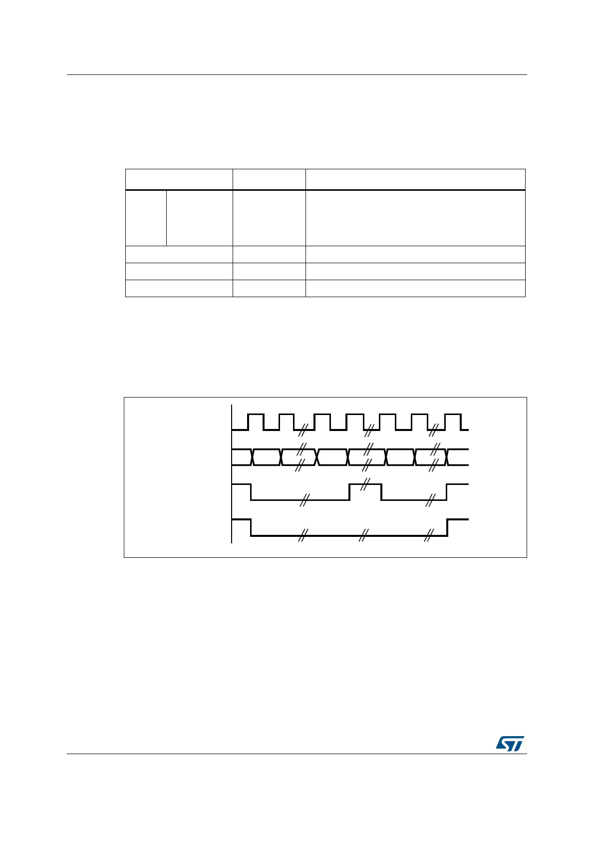
The data are synchronous with DCMI_PIXCLK and change on the rising/falling edge of the
pixel clock depending on the polarity.
The DCMI_HSYNC signal indicates the start/end of a line.
The DCMI_VSYNC signal indicates the start/end of a frame
Figure 148.DCMI signal waveforms
1. The capture edge of DCMI_PIXCLK is the falling edge, the active state of DCMI_HSYNC and
DCMI_VSYNC is 1.
2. DCMI_HSYNC and DCMI_VSYNC can change states at the same time.
8-bit data
When EDM[1:0] in DCMI_CR are programmed to “00” the interface captures 8 LSBs at its
input (DCMI_D[0:7]) and stores them as 8-bit data. The DCMI_D[13:8] inputs are ignored. In
this case, to capture a 32-bit word, the camera interface takes four pixel clock cycles.
The first captured data byte is placed in the LSB position in the 32-bit word and the 4
th
captured data byte is placed in the MSB position in the 32-bit word. Table 128 gives an
example of the positioning of captured data bytes in two 32-bit words.
Table 127.DCMI external signals
Signal name Signal type Signal description
8 bits
10 bits
12 bits
14 bits
DCMI_D[0..7]
DCMI_D[0..9]
DCMI_D[0..11]
DCMI_D[0..13]
Digital inputs DCMI data
DCMI_PIXCLK Digital input Pixel clock
DCMI_HSYNC Digital input Horizontal synchronization / Data valid
DCMI_VSYNC Digital input Vertical synchronization
$#-)?0)8#,+
$#-)?$2;=
$#-)?(39.#
$#-)?639.#
AIB
 Loading...


