Clock recovery system (CRS) (only valid for STM32L496xx/4A6xx devices) RM0351
280/1830 DocID024597 Rev 5
7.3 CRS functional description
7.3.1 CRS block diagram
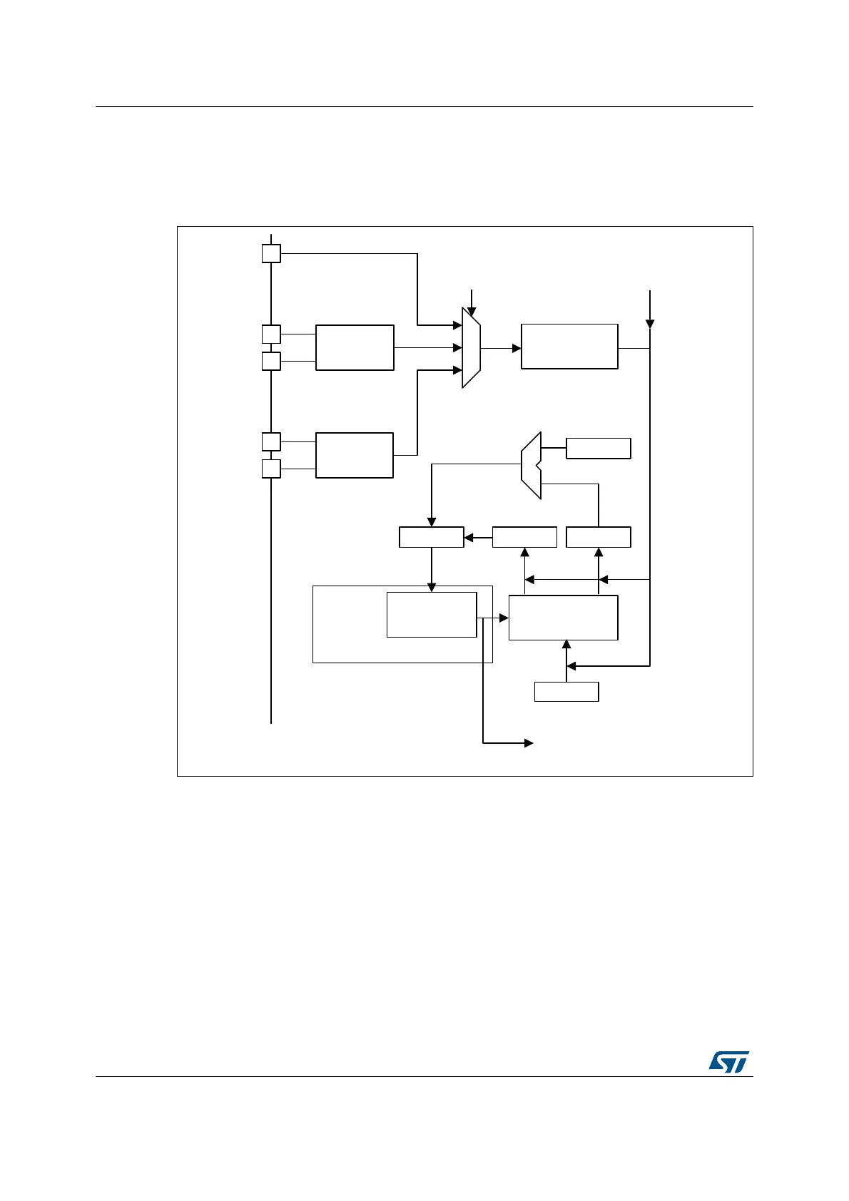
Figure 21. CRS block diagram
7.3.2 Synchronization input
The CRS synchronization (SYNC) source, selectable through the CRS_CFGR register, can
be the signal from the LSE clock or the USB SOF signal. For a better robustness of the
SYNC input, a simple digital filter (2 out of 3 majority votes, sampled by the RC48 clock) is
implemented to filter out any glitches. This source signal also has a configurable polarity
and can then be divided by a programmable binary prescaler to obtain a synchronization
signal in a suitable frequency range (usually around 1 kHz).
For more information on the CRS synchronization source configuration, refer to
Section 7.6.2: CRS configuration register (CRS_CFGR).
It is also possible to generate a synchronization event by software, by setting the SWSYNC
bit in the CRS_CR register.
06Y9
/6(
86%
6<1&65&
*3,2
26&B,1
26&B287
86%B'3
86%B'0
6<1&GLYLGHU
«
6:6<1&
5(/2$'
6<1&
ELWFRXQWHU
)(&$3
5&0+]
+6,
5&&
&56B6<1&
)(/,0
75,0 )(',5
7R86%
7R51*
 Loading...


