Analog-to-digital converters (ADC) RM0351
524/1830 DocID024597 Rev 5
Note: The regular trigger selection cannot be changed on-the-fly.
The injected trigger selection can be anticipated and changed on-the-fly. Refer to
Section 18.4.21: Queue of context for injected conversions on page 528
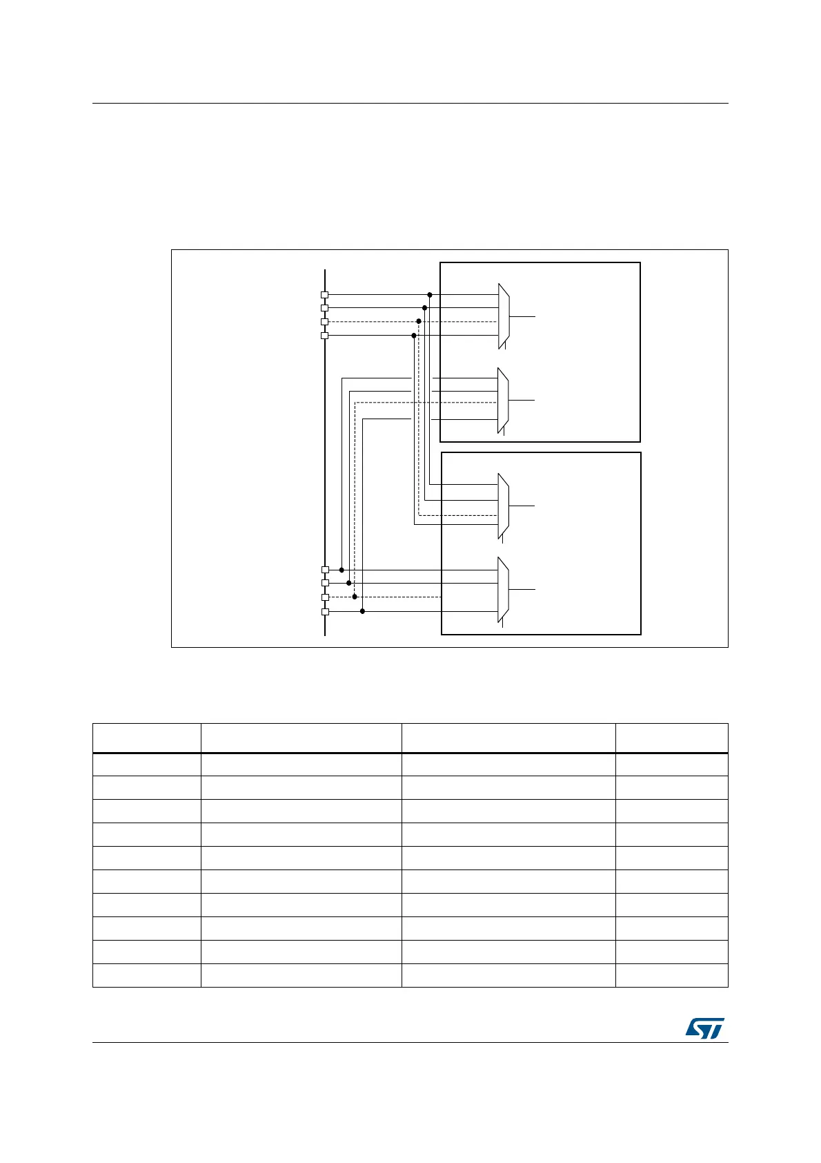
Each ADC master shares the same input triggers with its ADC slave as described in
Figure 78.
Figure 78. Triggers are shared between ADC master and ADC slave
Table 107 and Table 108 give all the possible external triggers of the three ADCs for regular
and injected conversion.
(;7
(;7
(;76(/>@
$'&0$67(5
(;7
-(;7
-(;7
,QMHFWHG
VHTXHQFHU
WULJJHUV
-(;7
-(;76(/>@
([WHUQDOUHJXODUWULJJHU
([WHUQDOLQMHFWHGWULJJHU
(;76(/>@
$'&6/$9(
-(;76(/>@
([WHUQDOUHJXODUWULJJHU
([WHUQDOLQMHFWHGWULJJHU
069
5HJXODU
VHTXHQFHU
WULJJHUV
Table 107. ADC1, ADC2 and ADC3 - External triggers for regular channels
Name Source Type EXTSEL[3:0]
EXT0 TIM1_CH1 Internal signal from on-chip timers 0000
EXT1 TIM1_CH2 Internal signal from on-chip timers 0001
EXT2 TIM1_CH3 Internal signal from on-chip timers 0010
EXT3 TIM2_CH2 Internal signal from on-chip timers 0011
EXT4 TIM3_TRGO Internal signal from on-chip timers 0100
EXT5 TIM4_CH4 Internal signal from on-chip timers 0101
EXT6 EXTI line 11 External pin 0110
EXT7 TIM8_TRGO Internal signal from on-chip timers 0111
EXT8 TIM8_TRGO2 Internal signal from on-chip timers 1000
EXT9 TIM1_TRGO Internal signal from on-chip timers 1001
 Loading...


