DocID024597 Rev 5 707/1830
RM0351 Digital filter for sigma delta modulators (DFSDM)
756
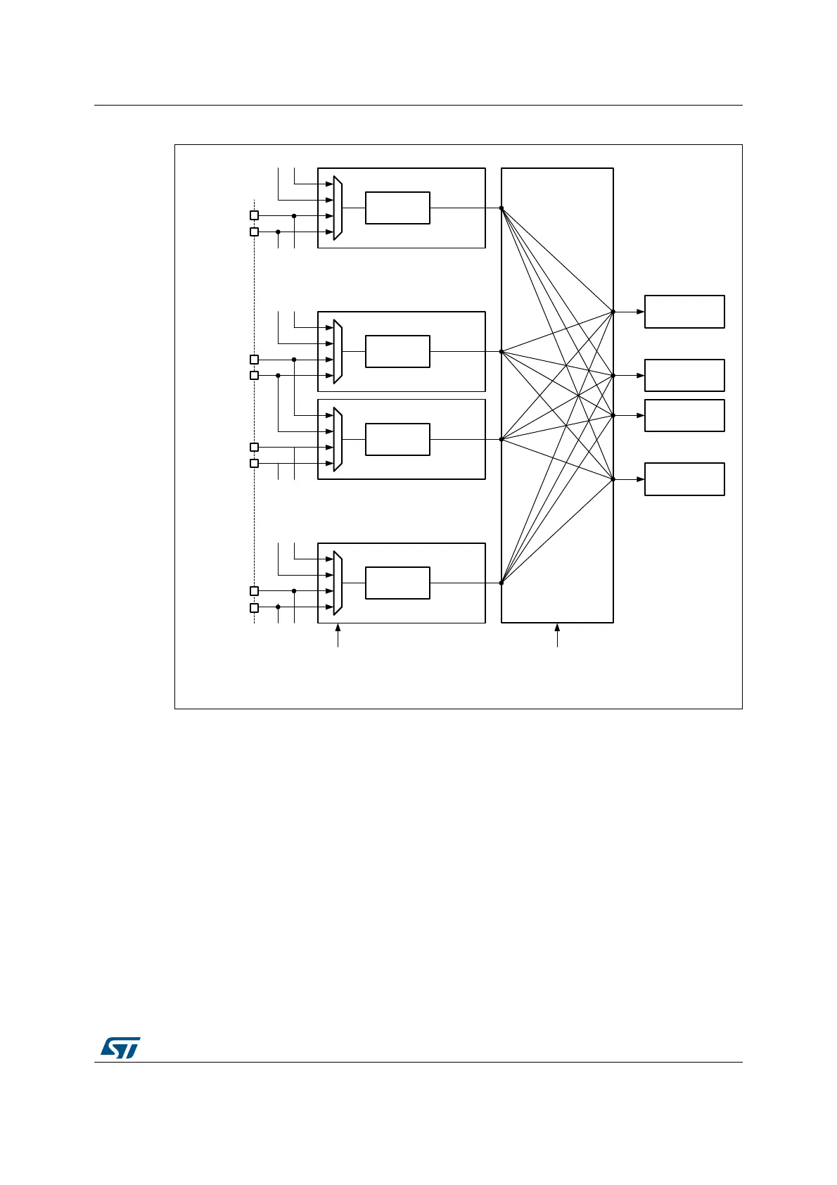
Figure 164. Input channel pins redirection
Output clock generation
A clock signal can be provided on CKOUT pin to drive external modulator clock inputs.
The frequency of this CKOUT signal is derived from DFSDM clock or from audio clock (see
CKOUTSRC bit in DFSDM_CH0CFGR1 register) divided by a predivider (see CKOUTDIV
bits in DFSDM_CH0CFGR1 register). If the output clock is stopped, then CKOUT signal is
set to low state (output clock can be stopped by CKOUTDIV=0 in DFSDM_CHyCFGR1
register or by DFSDMEN=0 in DFSDM_CH0CFGR1 register). The output clock stopping is
performed:
• 4 system clocks after DFSDMEN is cleared (if CKOUTSRC=0)
• 1 system clock and 3 audio clocks after DFSDMEN is cleared (if CKOUTSRC=1)
Before changing CKOUTSRC the software has to wait for CKOUT being stopped to avoid
glitch on CKOUT pin. The output clock signal frequency must be in the range 0 - 20 MHz.
06Y9
)/7[
)/7[
'$7$,1
'$7,1\
'$7,1\
'$7,1\
PD[
&+,16(/
5&+
)/7
)/7[
PD[
&.,1\
PD[
&.,1\
&.,1\
&.,1
&+\
PD[
'HFRGH
&+\
'HFRGH
&+\
'HFRGH
&+
'HFRGH
 Loading...


