Low-power timer (LPTIM) RM0351
1148/1830 DocID024597 Rev 5
34.4 LPTIM functional description
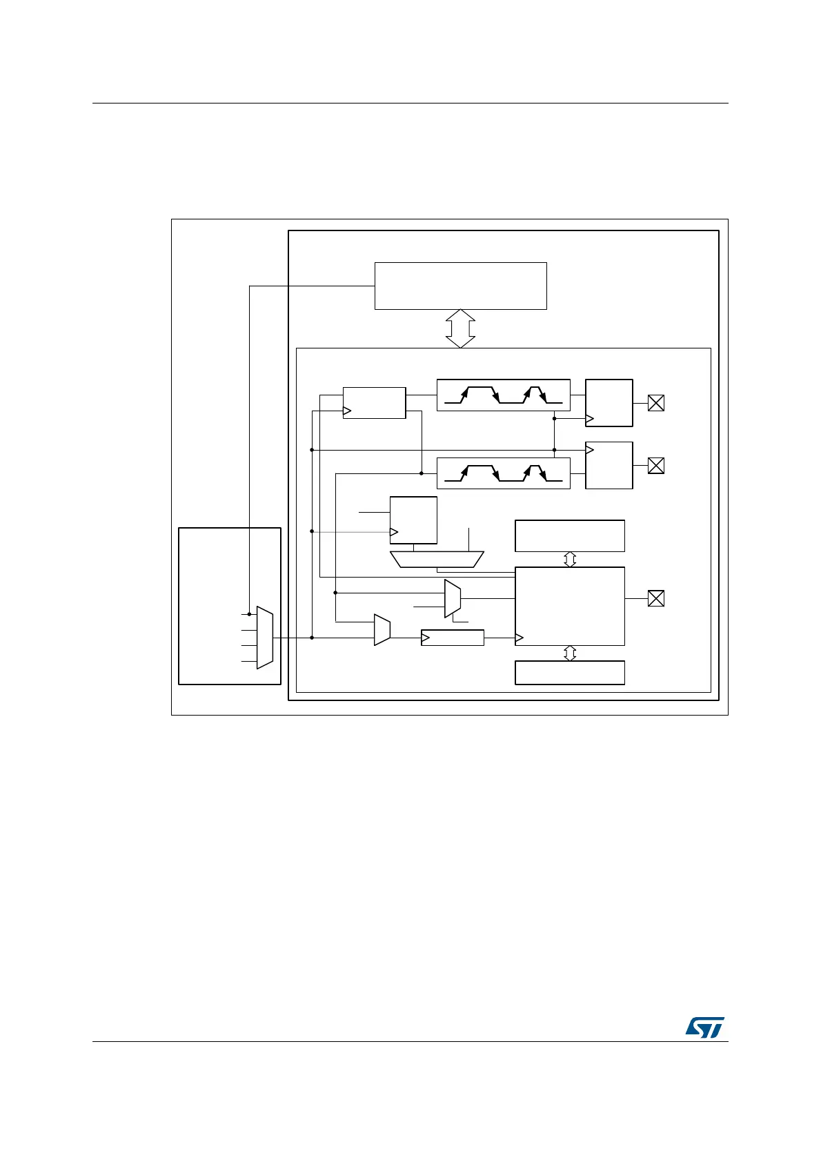
34.4.1 LPTIM block diagram
Figure 363. Low-power timer block diagram
34.4.2 LPTIM reset and clocks
The LPTIM can be clocked using several clock sources. It can be clocked using an internal
clock signal which can be chosen among APB, LSI, LSE or HSI16 sources through the
Clock Tree controller (RCC). Also, the LPTIM can be clocked using an external clock signal
injected on its external Input1. When clocked with an external clock source, the LPTIM may
run in one of these two possible configurations:
• The first configuration is when the LPTIM is clocked by an external signal but in the
same time an internal clock signal is provided to the LPTIM either from APB or any
other embedded oscillator including LSE, LSI and HSI16.
• The second configuration is when the LPTIM is solely clocked by an external clock
source through its external Input1. This configuration is the one used to realize Timeout
5&&
/37,0
$3%B,7)
.HUQHO
069
VZ
WULJJHU
XSWRH[W
WULJJHU
&/.08;
+6,
/6,
/6(
$3%FORFN
ELWFRPSDUH
ELWFRXQWHU
ELW$55
2XW
3UHVFDOHU
0X[WULJJHU
*OLWFK
ILOWHU
*OLWFK
ILOWHU
,QSXW
(QFRGHU
*OLWFK
ILOWHU
,QSXW
8SGRZQ
µ
&2817
02'(
 Loading...


