Comparator (COMP) RM0351
676/1830 DocID024597 Rev 5
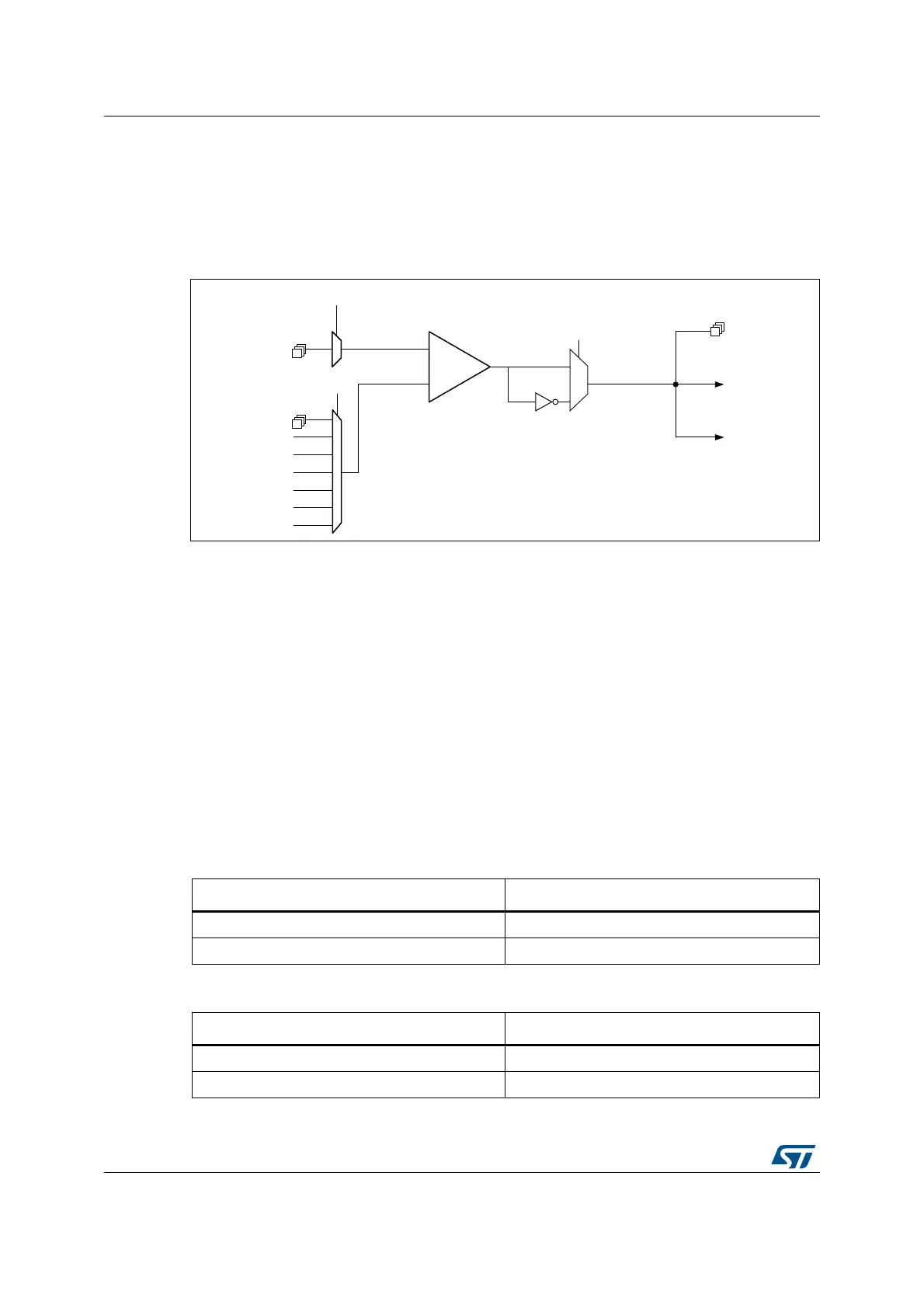
22.3 COMP functional description
22.3.1 COMP block diagram
The block diagram of the comparators is shown in Figure 155: Comparators block diagram.
Figure 155. Comparators block diagram
22.3.2 COMP pins and internal signals
The I/Os used as comparators inputs must be configured in analog mode in the GPIOs
registers.
The comparator output can be connected to the I/Os using the alternate function channel
given in “Alternate function mapping” table in the datasheet.
The output can also be internally redirected to a variety of timer input for the following
purposes:
• Emergency shut-down of PWM signals, using BKIN and BKIN2 inputs
• Cycle-by-cycle current control, using OCREF_CLR inputs
• Input capture for timing measures
It is possible to have the comparator output simultaneously redirected internally and
externally.
069
&203[B,10,2V
&203[B,13,2V
9
5(),17
9
5(),17
9
5(),17
9
5(),17
'$&B&+
'$&B&+
&203[B,13
&203[B,10
:DNHXS(;7,OLQH
LQWHUUXSW
3RODULW\VHOHFWLRQ
&203[B32/
&203[B9$/8(
&203[B287
&203[B
,106(/
7,0(56
*3,2
DOWHUQDWH
IXQFWLRQ
&203[
&203[B,136(/
Table 140. COMP1 input plus assignment
COMP1_INP COMP1_INPSEL
PC5 0
PB2 1
Table 141. COMP1 input minus assignment
COMP1_INM COMP1_INMSEL[2:0]
¼ V
REFINT
000
½ V
REFINT
001
 Loading...


