DocID024597 Rev 5 85/1830
RM0351
92
The data bus width is 36 bits because 4 bits are available for parity check (1 bit per byte) in
order to increase memory robustness, as required for instance by Class B or SIL norms.
The parity bits are computed and stored when writing into the SRAM2. Then, they are
automatically checked when reading. If one bit fails, an NMI is generated. The same error
can also be linked to the BRK_IN Break input of TIM1/TIM8/TIM15/TIM16/TIM17, with the
SPL control bit in the SYSCFG configuration register 2 (SYSCFG_CFGR2). The SRAM2
Parity Error flag (SPF) is available in the SYSCFG configuration register 2
(SYSCFG_CFGR2).
Note: When enabling the RAM parity check, it is advised to initialize by software the whole RAM
memory at the beginning of the code, to avoid getting parity errors when reading non-
initialized locations.
2.4.2 SRAM2 Write protection
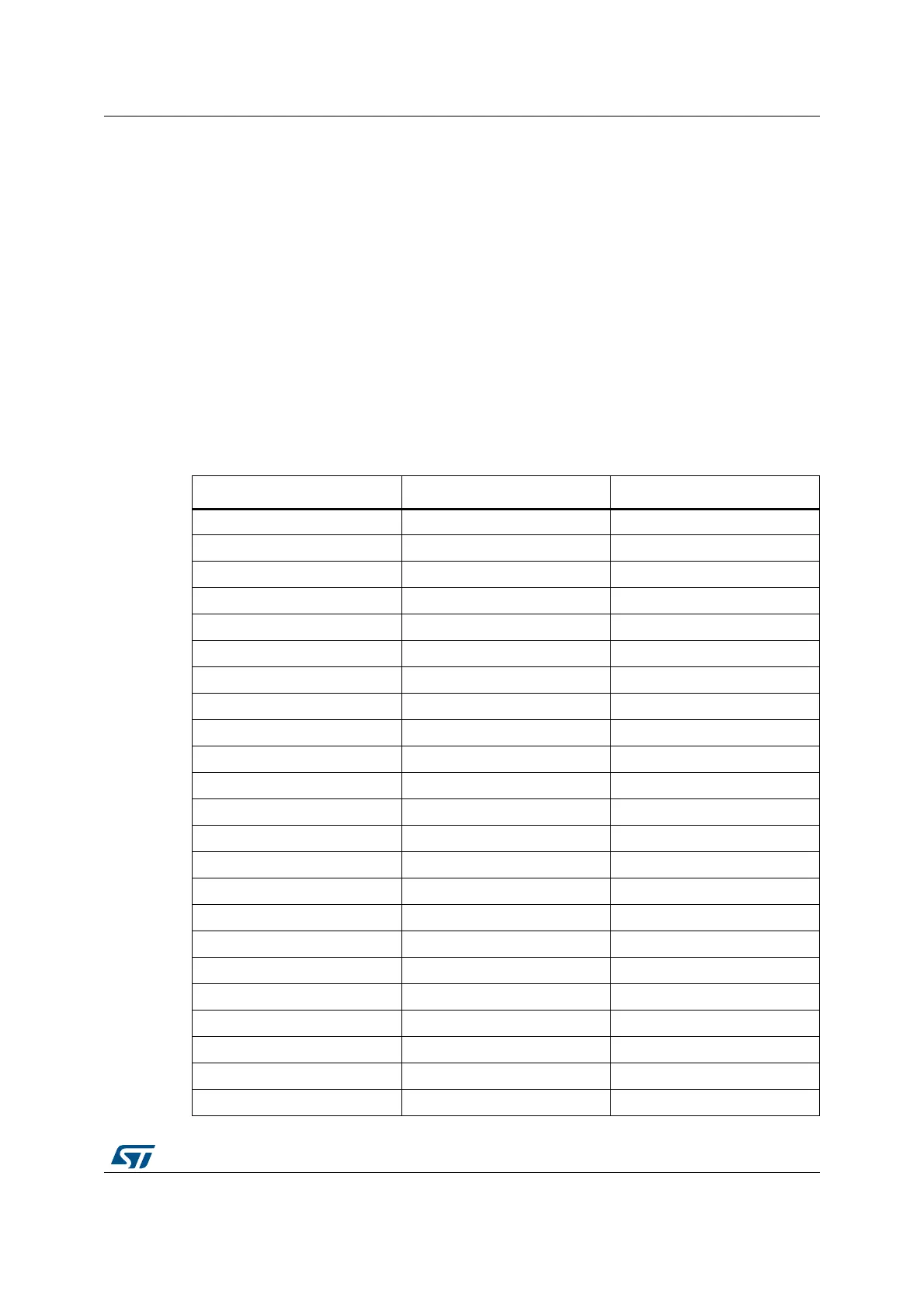
The SRAM2 can be write protected with a page granularity of 1 Kbyte.
Table 3. SRAM2 organization
Page number Start address End address
Page 0 0x1000 0000 0x1000 03FF
Page 1 0x1000 0400 0x1000 07FF
Page 2 0x1000 0800 0x1000 0BFF
Page 3 0x1000 0C00 0x1000 0FFF
Page 4 0x1000 1000 0x1000 13FF
Page 5 0x1000 1400 0x1000 17FF
Page 6 0x1000 1800 0x1000 1BFF
Page 7 0x1000 1C00 0x1000 1FFF
Page 8 0x1000 2000 0x1000 23FF
Page 9 0x1000 2400 0x1000 27FF
Page 10 0x1000 2800 0x1000 2BFF
Page 11 0x1000 2C00 0x1000 2FFF
Page 12 0x1000 3000 0x1000 33FF
Page 13 0x1000 3400 0x1000 37FF
Page 14 0x1000 3800 0x1000 3BFF
Page 15 0x1000 3C00 0x1000 3FFF
Page 16 0x1000 4000 0x1000 43FF
Page 17 0x1000 4400 0x1000 47FF
Page 18 0x1000 4800 0x1000 4BFF
Page 19 0x1000 4C00 0x1000 4FFF
Page 20 0x1000 5000 0x1000 53FF
Page 21 0x1000 5400 0x1000 57FF
Page 22 0x1000 5800 0x1000 5BFF

 Loading...