DocID024597 Rev 5 83/1830
RM0351
92
2.3 Bit banding
The Cortex
®
-M4 memory map includes two bit-band regions. These regions map each word
in an alias region of memory to a bit in a bit-band region of memory. Writing to a word in the
alias region has the same effect as a read-modify-write operation on the targeted bit in the
bit-band region.
In the STM32L4x6 devices both the peripheral registers and the SRAM1 are mapped to a
bit-band region, so that single bit-band write and read operations are allowed. The
operations are only available for Cortex
®
-M4 accesses, and not from other bus masters
(e.g. DMA).
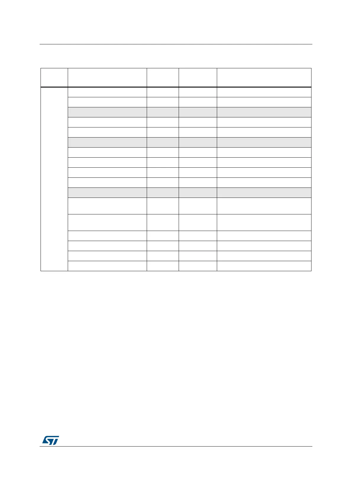
APB1
0x4000 4800 - 0x4000 4BFF 1 KB USART3 Section 40.8.12: USART register map
0x4000 4400 - 0x4000 47FF 1 KB USART2 Section 40.8.12: USART register map
0x4000 4000 - 0x4000 43FF 1KB Reserved -
0x4000 3C00 - 0x4000 3FFF 1 KB SPI3 Section 42.6.8: SPI register map
0x4000 3800 - 0x4000 3BFF 1 KB SPI2 Section 42.6.8: SPI register map
0x4000 3400 - 0x4000 37FF 1KB Reserved -
0x4000 3000 - 0x4000 33FF 1 KB IWDG Section 36.4.6: IWDG register map
0x4000 2C00 - 0x4000 2FFF 1 KB WWDG Section 37.4.4: WWDG register map
0x4000 2800 - 0x4000 2BFF 1 KB RTC Section 38.6.21: RTC register map
0x4000 2400 - 0x4000 27FF 1 KB LCD Section 25.6.6: LCD register map
0x4000 1800 - 0x4000 23FF 3KB Reserved -
0x4000 1400 - 0x4000 17FF 1 KB TIM7
Section 33.4.9: TIM6/TIM7 register
map
0x4000 1000 - 0x4000 13FF 1 KB TIM6
Section 33.4.9: TIM6/TIM7 register
map
0x4000 0C00- 0x4000 0FFF 1 KB TIM5 Section 31.4.23: TIMx register map
0x4000 0800 - 0x4000 0BFF 1 KB TIM4 Section 31.4.23: TIMx register map
0x4000 0400 - 0x4000 07FF 1 KB TIM3 Section 31.4.23: TIMx register map
0x4000 0000 - 0x4000 03FF 1 KB TIM2 Section 31.4.23: TIMx register map
1. The gray color is used for reserved boundary addresses.
Table 2. STM32L496xx/4A6xx devices memory map and peripheral register boundary
addresses
(1)
(continued)
Bus Boundary address
Size
(bytes)
Peripheral Peripheral register map
 Loading...


