USB on-the-go full-speed (OTG_FS) RM0351
1650/1830 DocID024597 Rev 5
Data FIFO (DFIFO) access register map
These registers, available in both host and device modes, are used to read or write the FIFO
space for a specific endpoint or a channel, in a given direction. If a host channel is of type
IN, the FIFO can only be read on the channel. Similarly, if a host channel is of type OUT, the
FIFO can only be written on the channel.
Power and clock gating CSR map
There is a single register for power and clock gating. It is available in both host and device
modes.
47.15 OTG_FS registers
These registers are available in both host and device modes, and do not need to be
reprogrammed when switching between these modes.
Bit values in the register descriptions are expressed in binary unless otherwise specified.
47.15.1 OTG control and status register (OTG_GOTGCTL)
Address offset: 0x000
Reset value: 0x0X01 0000
The OTG_GOTGCTL register controls the behavior and reflects the status of the OTG
function of the core.
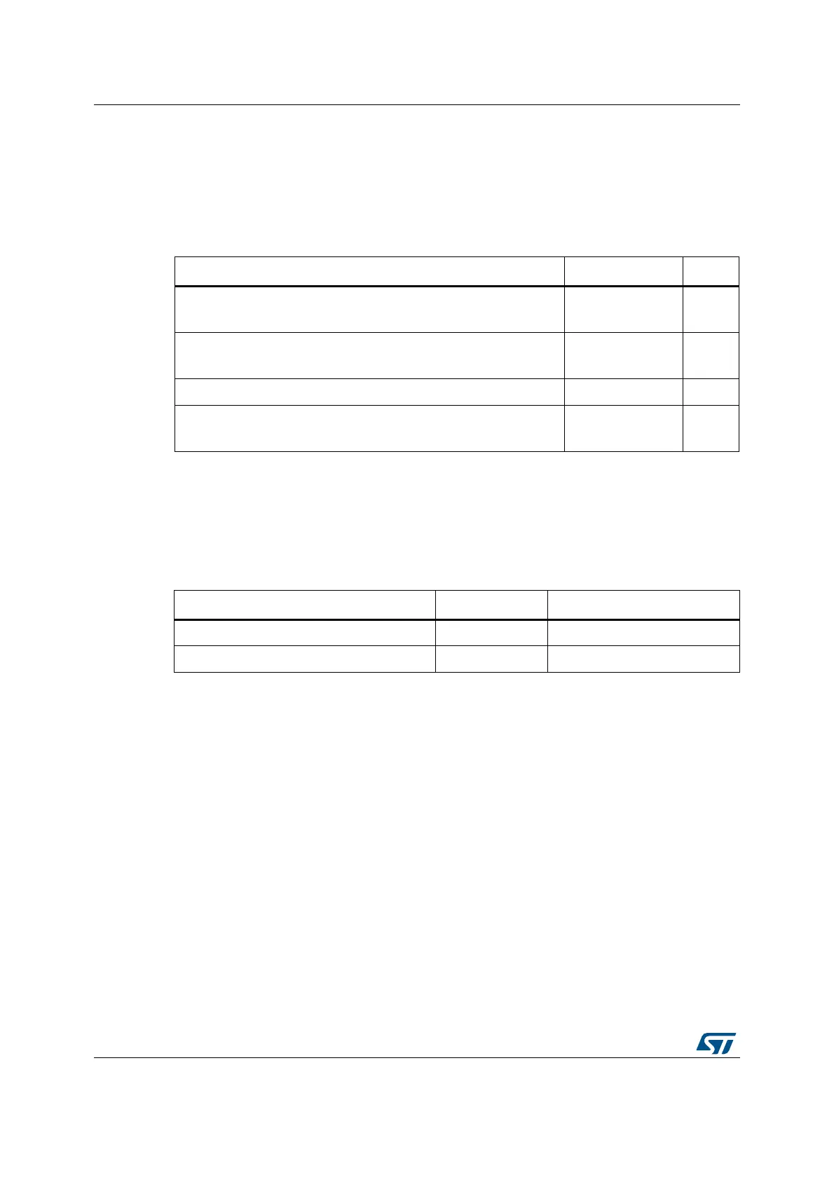
Table 305. Data FIFO (DFIFO) access register map
FIFO access register section Address range Access
Device IN Endpoint 0/Host OUT Channel 0: DFIFO Write Access
Device OUT Endpoint 0/Host IN Channel 0: DFIFO Read Access
0x1000–0x1FFC
w
r
Device IN Endpoint 1/Host OUT Channel 1: DFIFO Write Access
Device OUT Endpoint 1/Host IN Channel 1: DFIFO Read Access
0x2000–0x2FFC
w
r
... ... ...
Device IN Endpoint x
(1)
/Host OUT Channel x
(1)
: DFIFO Write Access
Device OUT Endpoint x
(1)
/Host IN Channel x
(1)
: DFIFO Read Access
1. Where x is 5 in device mode and 11 in host mode.
0xX000–0xXFFC
w
r
Table 306. Power and clock gating control and status registers
Register name Acronym Offset address: 0xE00–0xFFF
Power and clock gating control register PCGCCTL 0xE00-0xE04
Reserved - 0xE05–0xFFF
 Loading...


