Reset and clock control (RCC) RM0351
270/1830 DocID024597 Rev 5
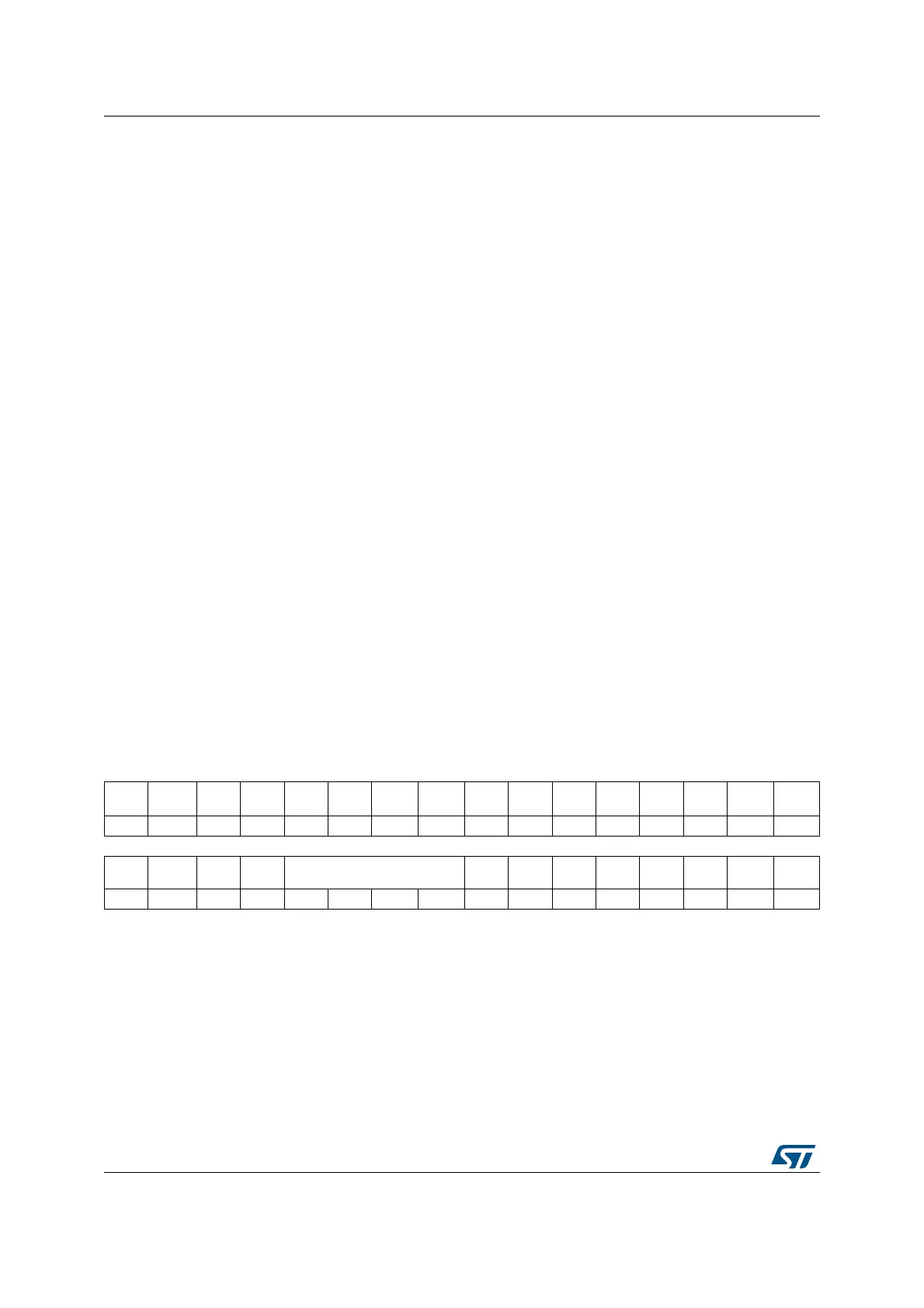
6.4.30 Control/status register (RCC_CSR)
Address: 0x94
Reset value: 0x0C00 0600, reset by system Reset, except reset flags by power Reset only.
Access: 0 wait state 3, word, half-word and byte access
Wait states are inserted in case of successive accesses to this register.
Bits 4:3 LSEDRV[1:0] LSE oscillator drive capability
Set by software to modulate the LSE oscillator’s drive capability.
00: ‘Xtal mode’ lower driving capability
01: ‘Xtal mode’ medium low driving capability
10: ‘Xtal mode’ medium high driving capability
11: ‘Xtal mode’ higher driving capability
The oscillator is in Xtal mode when it is not in bypass mode.
Bit 2 LSEBYP: LSE oscillator bypass
Set and cleared by software to bypass oscillator in debug mode. This bit can be written only
when the external 32 kHz oscillator is disabled (LSEON=0 and LSERDY=0).
0: LSE oscillator not bypassed
1: LSE oscillator bypassed
Bit 1 LSERDY: LSE oscillator ready
Set and cleared by hardware to indicate when the external 32 kHz oscillator is stable. After
the LSEON bit is cleared, LSERDY goes low after 6 external low-speed oscillator clock
cycles.
0: LSE oscillator not ready
1: LSE oscillator ready
Bit 0 LSEON: LSE oscillator enable
Set and cleared by software.
0: LSE oscillator OFF
1: LSE oscillator ON
31 30 29 28 27 26 25 24 23 22 21 20 19 18 17 16
LPWR
RSTF
WWDG
RSTF
IWWG
RSTF
SFT
RSTF
BOR
RSTF
PIN
RSTF
OBL
RSTF
FW
RSTF
RMVF Res. Res. Res. Res. Res. Res. Res.
r r rrrr r rrw
1514131211109 8765432 1 0
Res. Res. Res. Res. MSISRANGE[3:0] Res. Res. Res. Res. Res. Res.
LSI
RDY
LSION
rw rw rw rw r rw
 Loading...


