Advanced-control timers (TIM1/TIM8) RM0351
960/1830 DocID024597 Rev 5
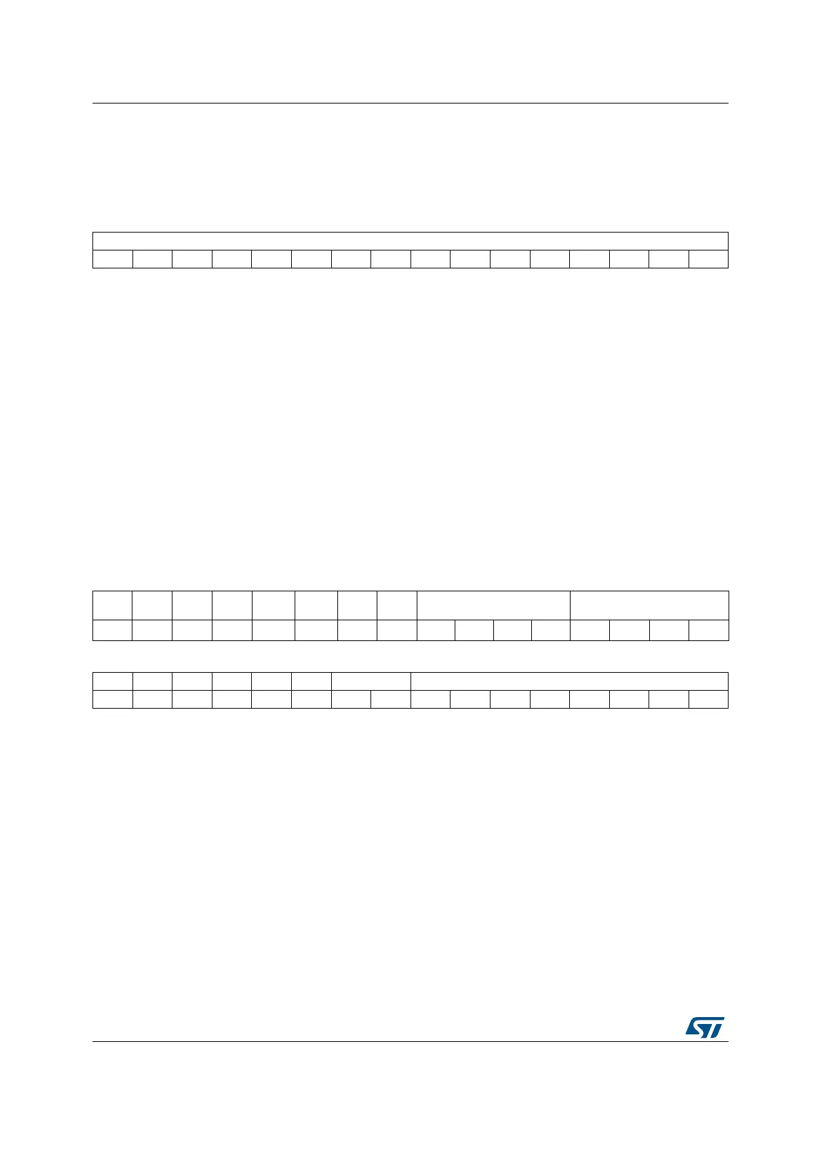
30.4.17 TIM1/TIM8 capture/compare register 4 (TIMx_CCR4)
Address offset: 0x40
Reset value: 0x0000
30.4.18 TIM1/TIM8 break and dead-time register (TIMx_BDTR)
Address offset: 0x44
Reset value: 0x0000 0000
Note: As the bits BK2P, BK2E, BK2F[3:0], BKF[3:0], AOE, BKP, BKE, OSSI, OSSR and DTG[7:0]
can be write-locked depending on the LOCK configuration, it can be necessary to configure
all of them during the first write access to the TIMx_BDTR register.
1514131211109876543210
CCR4[15:0]
rw/r rw/r rw/r rw/r rw/r rw/r rw/r rw/r rw/r rw/r rw/r rw/r rw/r rw/r rw/r rw/r
Bits 15:0 CCR4[15:0]: Capture/Compare value
If channel CC4 is configured as output: CCR4 is the value to be loaded in the actual
capture/compare 4 register (preload value).
It is loaded permanently if the preload feature is not selected in the TIMx_CCMR2 register
(bit OC4PE). Else the preload value is copied in the active capture/compare 4 register when
an update event occurs.
The active capture/compare register contains the value to be compared to the counter
TIMx_CNT and signalled on OC4 output.
If channel CC4 is configured as input: CCR4 is the counter value transferred by the last
input capture 4 event (IC4). The TIMx_CCR4 register is read-only and cannot be
programmed.
31 30 29 28 27 26 25 24 23 22 21 20 19 18 17 16
R e s. Res. Res. Res.
Res. Res.
BK2P BK2E BK2F[3:0] BKF[3:0]
rw rw rw rw rw rw rw rw rw rw
1514131211109876543210
MOE AOE BKP BKE OSSR OSSI LOCK[1:0] DTG[7:0]
rw rw rw rw rw rw rw rw rw rw rw rw rw rw rw rw
Bits 31:26 Reserved, must be kept at reset value.
Bit 25 BK2P: Break 2 polarity
0: Break input BRK2 is active low
1: Break input BRK2 is active high
Note: This bit cannot be modified as long as LOCK level 1 has been programmed (LOCK bits
in TIMx_BDTR register).
Note: Any write operation to this bit takes a delay of 1 APB clock cycle to become effective.
 Loading...


