Refer to Arria 10 Register Map for details on the specific registers that set the
CTLE gain values/DFE taps.
b. For dynamically changing DFE and CTLE Adaptation modes, refer to CTLE
Settings in Triggered Adaptation Mode, Arria 10 Register Map and Arria 10
DFE Adaptation Tool for the list of adaptation registers. Use the
reconfiguration interface to change the register settings.
Note: You must set VGA manually for all combinations of CTLE mode and DFE
modes.
Related Information
• CTLE Settings in Triggered Adaptation Mode
• Arria 10 Register Map
Arria 10 DFE Adaptation Tool is a separate tab in the Arria 10 Register Map.
5.1.2.2. Clock Data Recovery (CDR) Unit
The PMA of each channel includes a channel PLL that you can configure as a receiver
clock data recovery (CDR) for the receiver. You can also configure the channel PLL of
channels 1 and 4 as a clock multiplier unit (CMU) PLL for the transmitter in the same
bank.
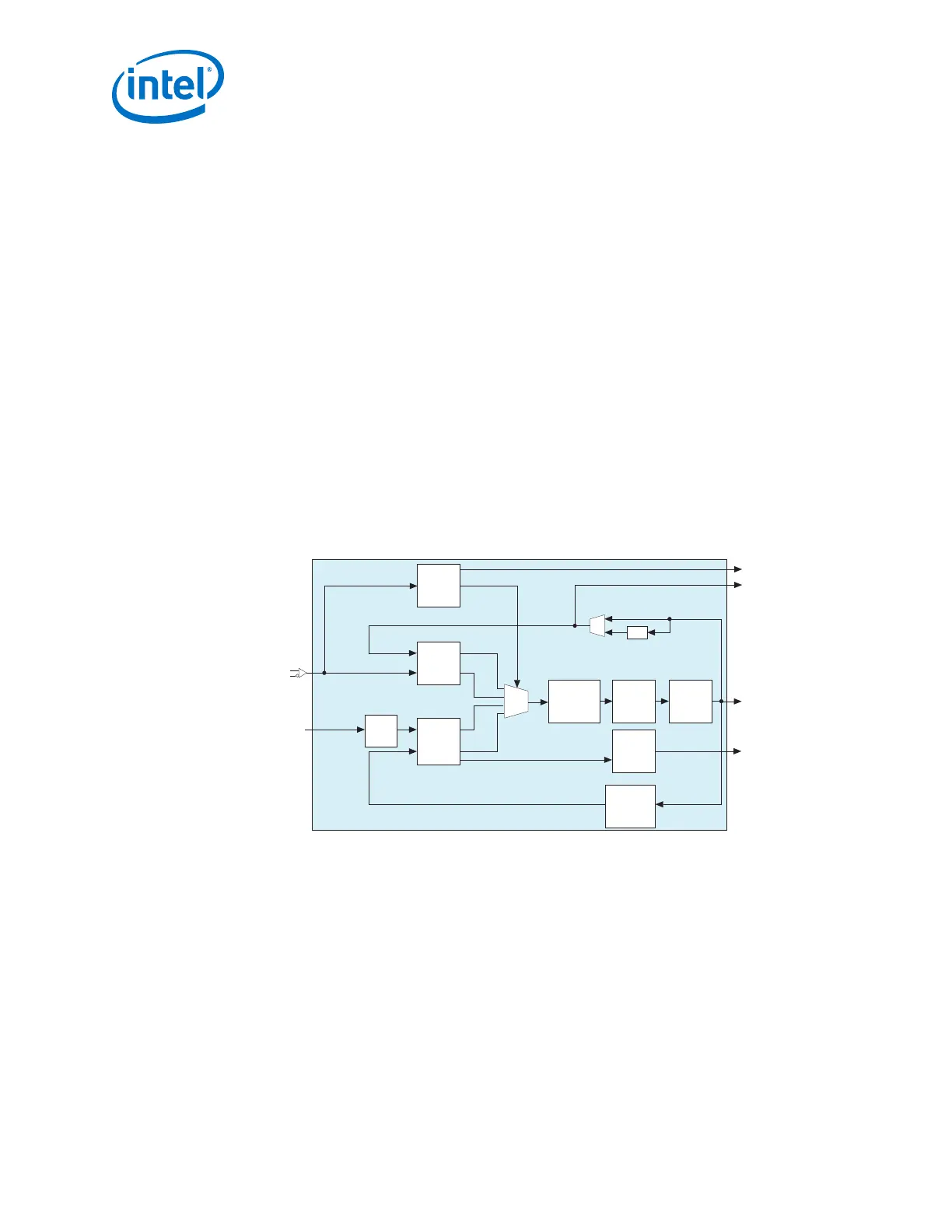
Figure 231. Channel PLL Configured as CDR
Serial Clock
rx_is_lockedtoref
rx_serial_data
refclk
Recovered Clock
LTR/LTD
Controller
Phase
Detector
(PD)
Down
Up
Up
Down
Charge Pump
&
Loop Filter
Voltage
Controlled
Oscillator
(VCO)
Lock
Detect
Phase
Frequency
Detector
(PFD)
/2
Channel PLL
M
Divider
(1)
Note:
1. The Quartus® Prime Pro Edition software automatically chooses the optimal values.
rx_is_lockedtodata
N
Divider
(1)
L
Divider
(1)
5.1.2.2.1. Lock-to-Reference Mode
In LTR mode, the phase frequency detector (PFD) in the CDR tracks the receiver input
reference clock. The PFD controls the charge pump that tunes the VCO in the CDR.
The rx_is_lockedtoref status signal is asserted active high to indicate that the
CDR has locked to the phase and frequency of the receiver input reference clock.
Note:
The phase detector (PD) is inactive in LTR mode.
5. Arria 10 Transceiver PHY Architecture
UG-01143 | 2018.06.15
Intel
®
Arria
®
10 Transceiver PHY User Guide
458