RTC6 boards
Doc. Rev. 1.0.21 en-US
2 Product Overview
41
Notes for RTC5 Users
• In contrast to RTC5 boards, jumper numbers are
no longer imprinted on RTC6 PCIe Boards.
Therefore, RTC5 jumper designations cannot
longer be used in this RTC6 Manual. The relation
of the designations establishes Figure 1.
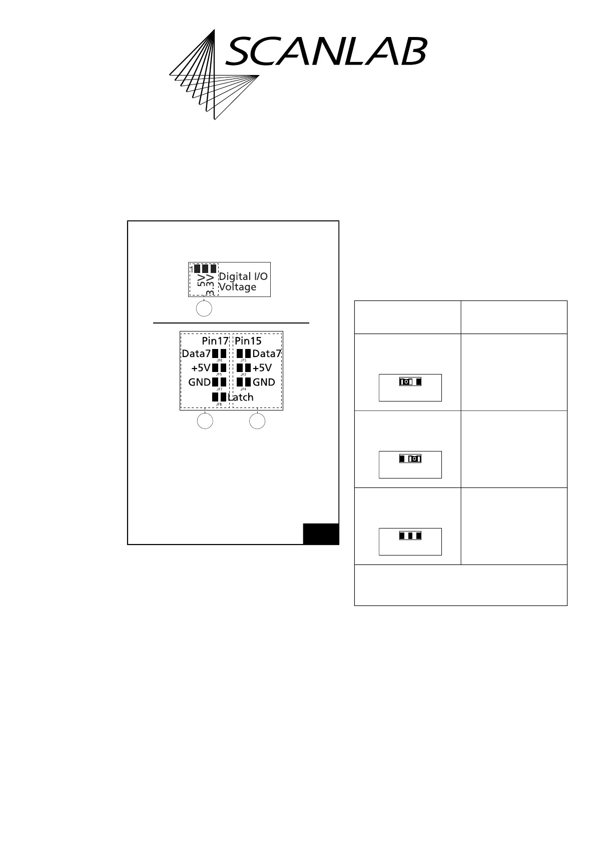
2.7.1 Solder Jumper Field A –
Configuring Output Signal
Level at EXTENSION 1 Socket
Connector
The solder jumper field A is located on the lower side
of the RTC6 PCIe Board, see Figure 6.
It is used to set the level (5 V or 3.3 V) of all output
signals at the EXTENSION 1 socket connector, see the
following table.
See also Section ”Configuring the Output Signal
Level”, page 78.
1
Jumper designations with RTC5 boards and
RTC6 PCIe Boards.
Figure shows RTC5 board.
3
2
1
RTC5: JP4
RTC5: JP2
RTC5: JP3
RTC5: JP8
RTC5: JP7
RTC5: JP5
RTC5: JP6
RTC5: JP1
Legend
1. With RTC6 PCIe Boards referred to as
solder jumper field A in this manual
(1)
.
2. With RTC6 PCIe Boards referred to as
solder jumper field B in this manual
(3)
.
3. With RTC6 PCIe Boards referred to as
solder jumper field C in this manual
(2)
.
RTC5 Boards
Allowed
jumper setting
EXTENSION 1
socket connector
Output signal level
5 V.
Output signal level
3.3 V.
No signal output.
*
Caution: make sure that only one position is closed
in this solder jumper field. Other combinations are
not allowed and cause damage to the board!
closed*
open
Digital I/O Voltage
3.3V5V
open
closed*
Digital I/O Voltage
3.3V5V
open
open
Digital I/O Voltage
3.3V5V