RTC6 boards
Doc. Rev. 1.0.21 en-US
4 RTC6 PCIe Board – Layout and Interfaces
65
4.2 Layout – Lower Side
6
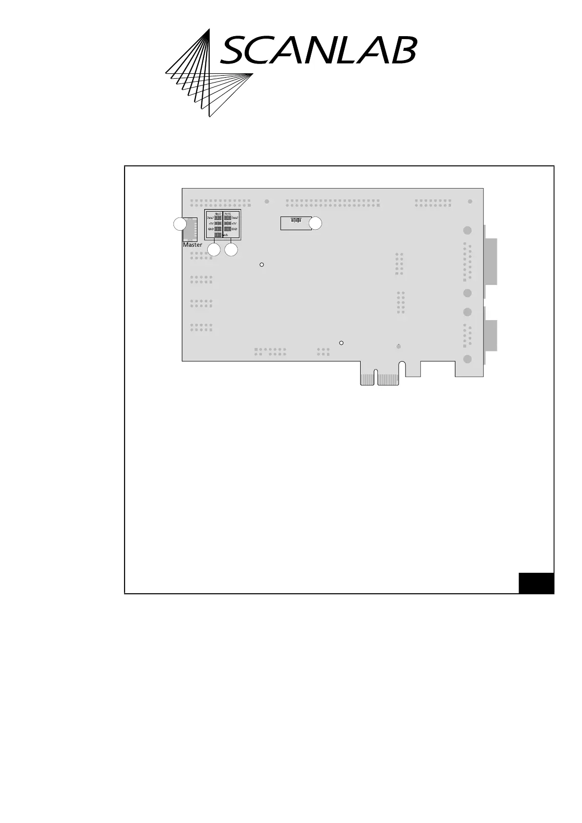
RTC6 PCIe Board: lower side.
Digital I/O Voltage
3.3V5V
4
3
2
1
Legend
1. Master . . . . . . . . . . . . . . 6-pin socket connector. To connect with another RTC6 PCIe Board for clock synchronization.
For details, see Chapter 4.4 ”Master Socket Connector, Slave Socket Connector”, page 66.
2. Solder jumper field A. . . To configure the level of the output signals at the EXTENSION 1 socket connector. For
details, see “Solder Jumper Field A – Configuring Output Signal Level at EXTENSION 1
Socket Connector”, page 41.
3. Solder jumper field B . . . To configure the signal at EXTENSION 2 socket connector pin (17). For details, see “Solder
Jumper Field B – Configuring Pin (17) of EXTENSION 2 Socket Connector”, page 42.
4. Solder jumper field C . . . To configure the signal at EXTENSION 2 socket connector pin (15). For details, see “Solder
Jumper Field C – Configuring Pin (15) of EXTENSION 2 Socket Connector”, page 43.