DocID024597 Rev 5 1699/1830
RM0351 USB on-the-go full-speed (OTG_FS)
1774
47.15.39 OTG device V
BUS
discharge time register
(OTG_DVBUSDIS)
Address offset: 0x0828
Reset value: 0x0000 17D7
This register specifies the V
BUS
discharge time after V
BUS
pulsing during SRP.
47.15.40 OTG device V
BUS
pulsing time register
(OTG_DVBUSPULSE)
Address offset: 0x082C
Reset value: 0x0000 05B8
This register specifies the V
BUS
pulsing time during SRP.
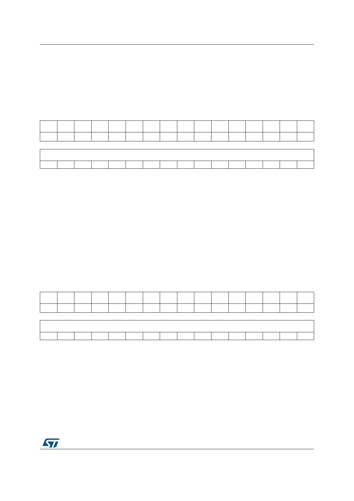
31 30 29 28 27 26 25 24 23 22 21 20 19 18 17 16
Res. Res. Res. Res. Res. Res. Res. Res. Res. Res. Res. Res. Res. Res. Res. Res.
1514131211109876543210
VBUSDT
rw rw rw rw rw rw rw rw rw rw rw rw rw rw rw rw
Bits 31:16 Reserved, must be kept at reset value.
Bits 15:0 VBUSDT: Device V
BUS
discharge time
Specifies the V
BUS
discharge time after V
BUS
pulsing during SRP. This value equals:
V
BUS
discharge time in PHY clocks / 1 024
Depending on your V
BUS
load, this value may need adjusting.
31 30 29 28 27 26 25 24 23 22 21 20 19 18 17 16
Res. Res. Res. Res. Res. Res. Res. Res. Res. Res. Res. Res. Res. Res. Res. Res.
1514131211109876543210
DVBUSP
rw rw rw rw rw rw rw rw rw rw rw rw rw rw rw rw
Bits 31:12 Reserved, must be kept at reset value.
Bits 11:0 DVBUSP: Device V
BUS
pulsing time
Specifies the V
BUS
pulsing time during SRP. This value equals:
V
BUS
pulsing time in PHY clocks / 1 024
 Loading...


