Reset and clock control (RCC) RM0351
240/1830 DocID024597 Rev 5
6.4.12 AHB3 peripheral reset register (RCC_AHB3RSTR)
Address offset: 0x30
Reset value: 0x00000 0000
Access: no wait state, word, half-word and byte access
6.4.13 APB1 peripheral reset register 1 (RCC_APB1RSTR1)
Address offset: 0x38
Reset value: 0x0000 0000
Access: no wait state, word, half-word and byte access
Bit 2 GPIOCRST: IO port C reset
Set and cleared by software.
0: No effect
1: Reset IO port C
Bit 1 GPIOBRST: IO port B reset
Set and cleared by software.
0: No effect
1: Reset IO port B
Bit 0 GPIOARST: IO port A reset
Set and cleared by software.
0: No effect
1: Reset IO port A
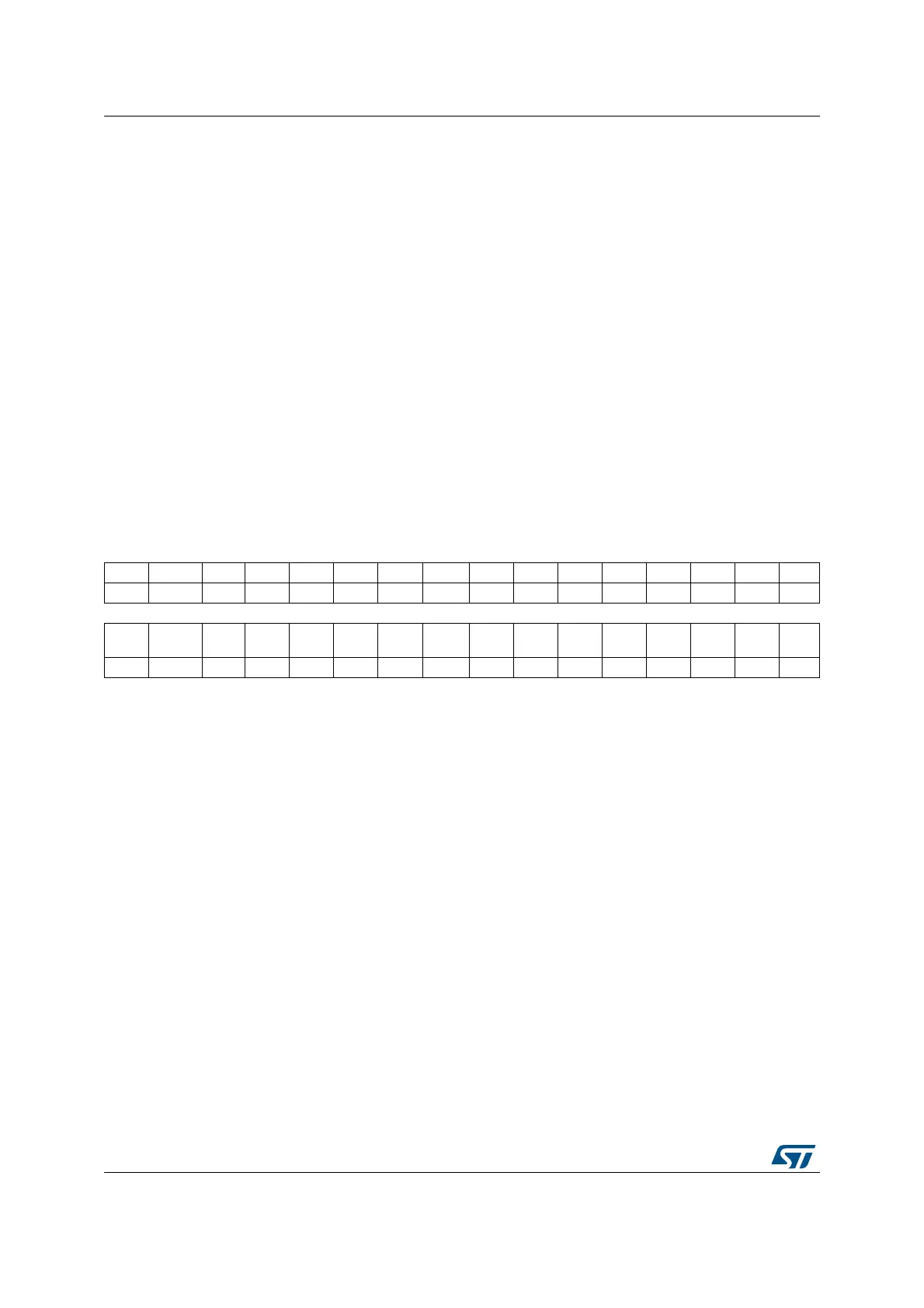
31 30 29 28 27 26 25 24 23 22 21 20 19 18 17 16
Res. Res. Res. Res. Res. Res. Res. Res. Res. Res. Res. Res. Res. Res. Res. Res.
1514131211109 8 76543210
Res. Res. Res. Res. Res. Res. Res.
QSPI
RST
Res. Res. Res. Res. Res. Res. Res.
FMC
RST
rw rw
Bits 31:9 Reserved, must be kept at reset value.
Bit 8 QSPIRST: QUADSPI1 memory interface reset
Set and cleared by software.
0: No effect
1: Reset QUADSPI
Bits 7:1 Reserved, must be kept at reset value.
Bit 0 FMCRST: Flexible memory controller reset
Set and cleared by software.
0: No effect
1: Reset FMC
 Loading...


