RTC6 boards
Doc. Rev. 1.0.21 en-US
4 RTC6 PCIe Board – Layout and Interfaces
77
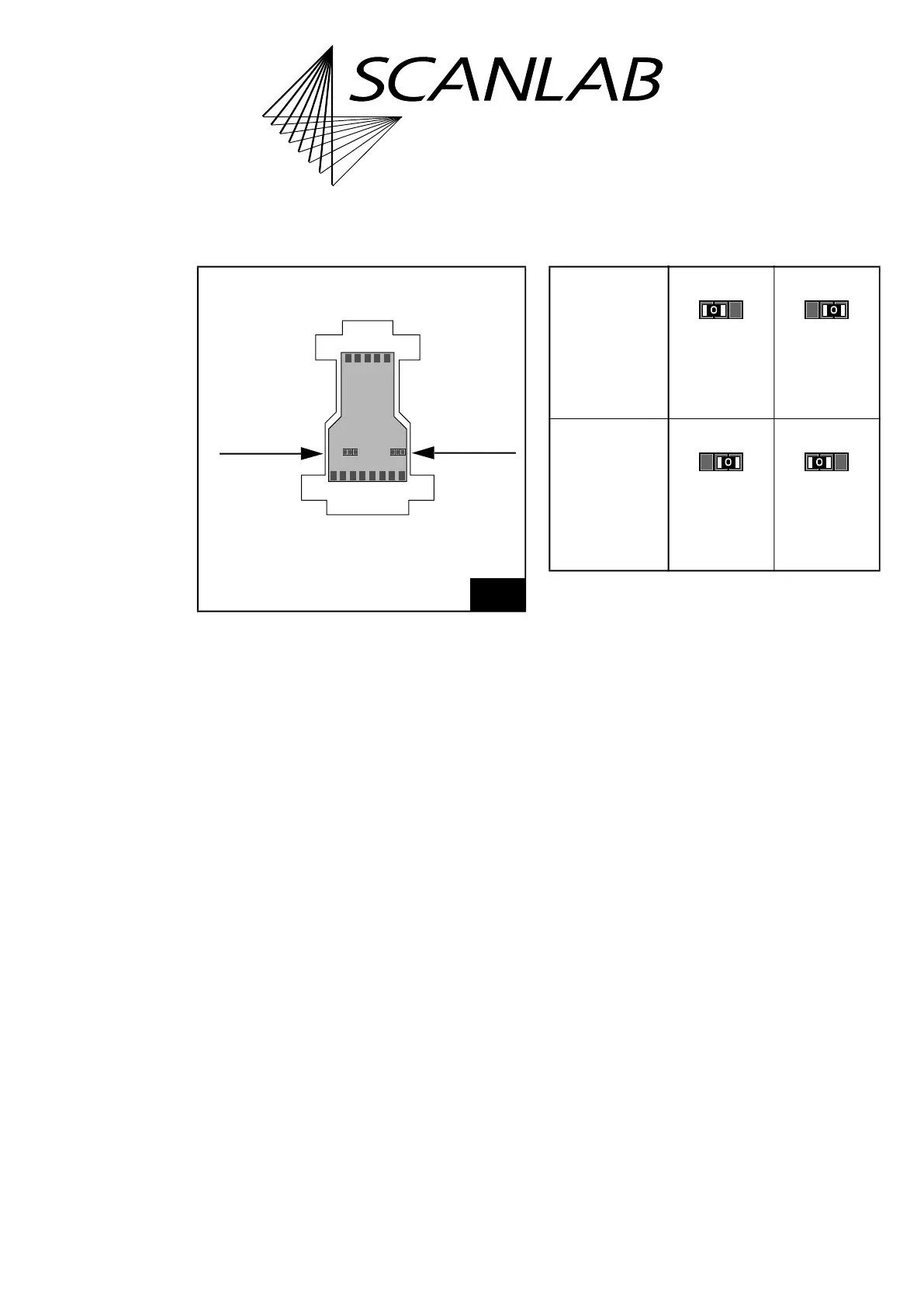
The positions of the solder jumpers on the PCB is
shown in Figure 21.
The following table shows the possible jumper
settings. Other jumper settings are not allowed.
21
Laser adapter (accessory): position of solder jumper
JP1 and JP2 on the printed circuit board.
1
ANA1
PIN4
+5V
ANA2
PIN2
LON
JP2JP1
1
Solder jumper
JP1:
signal at
pin (02)
Position 1-2
LASERON
(default
configuration)
Position 2-3
ANALOG OUT2
Solder jumper
JP2:
signal at
pin (04)
Position 1-2
ANALOG OUT1
(default
configuration)
Position 2-3
+5 V
1
ANA2
PIN2
LON
1
ANA1
PIN4
+5V