RM0008 Analog-to-digital converter (ADC)
151/690
10.3.1 ADC on-off control
The ADC can be powered-on by setting the ADON bit in the ADC_CR2 register. When the
ADON bit is set for the first time, it wakes up the ADC from Power Down mode.
Conversion starts when ADON bit is set for a second time by software after ADC power-up
time (t
STAB
).
You can stop conversion and put the ADC in power down mode by resetting the ADON bit. In
this mode the ADC consumes almost no power (only a few µA).
10.3.2 ADC clock
The ADCCLK clock provided by the Clock Controller is synchronous with the PCLK2 (APB2
clock). The RCC controller has a dedicated programmable prescaler for the ADC clock, refer
to Reset and clock control (RCC) on page 69
for more details.
10.3.3 Channel selection
There are 16 multiplexed channels. It is possible to organize the conversions in two groups:
regular and injected. A group consists of a sequence of conversions which can be done on
any channel and in any order. For instance, it is possible to do the conversion in the
following order: Ch3, Ch8, Ch2, Ch2, Ch0, Ch2, Ch2, Ch15.
● The regular group is composed of up to 16 conversions. The regular channels and
their order in the conversion sequence must be selected in the ADC_SQRx registers.
The total number of conversions in the regular group must be written in the L[3:0] bits in
the ADC_SQR1 register.
● The injected group is composed of up to 4 conversions. The injected channels and
their order in the conversion sequence must be selected in the ADC_JSQR register.
The total number of conversions in the injected group must be written in the L[1:0] bits
in the ADC_JSQR register.
If the ADC_SQRx or ADC_JSQR registers are modified during a conversion, the current
conversion is reset and a new start pulse is sent to the ADC to convert the new chosen
group.
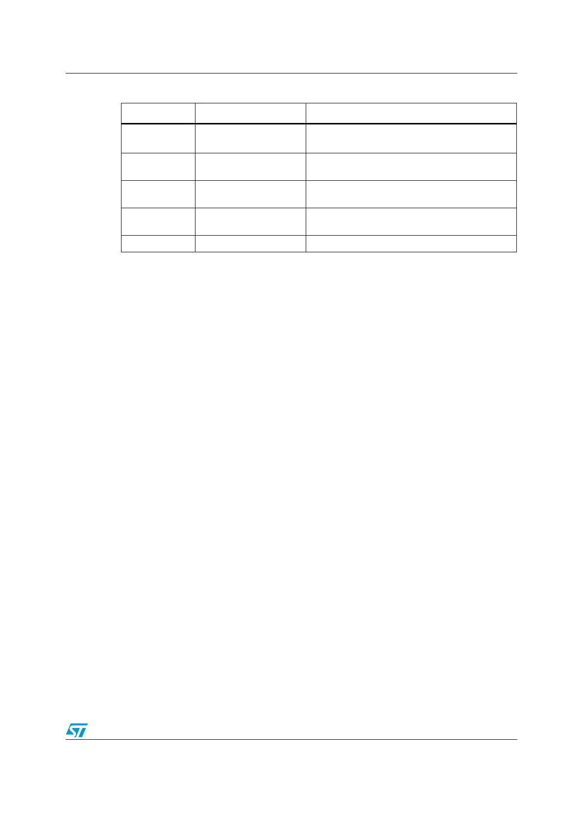
Table 42. ADC pins
Name Signal type Remarks
V
REF+
Input, analog reference
positive
The higher/positive reference voltage for the ADC,
2.4 V
≤ V
REF+
≤ V
DDA
V
DDA
Input, analog supply
Analog power supply equal to V
DD
and
2.4 V ≤ V
DDA
≤ V
DD
(3.6 V)
V
REF-
Input, analog reference
negative
The lower/negative reference voltage for the ADC,
V
REF-
=
V
SSA
V
SSA
Input, analog supply
ground
Ground for analog power supply equal to V
SS
ADCx_IN[15:0] Analog input signals 16 analog input channels
 Loading...


