Flexible static memory controller (FSMC) RM0008
404/690
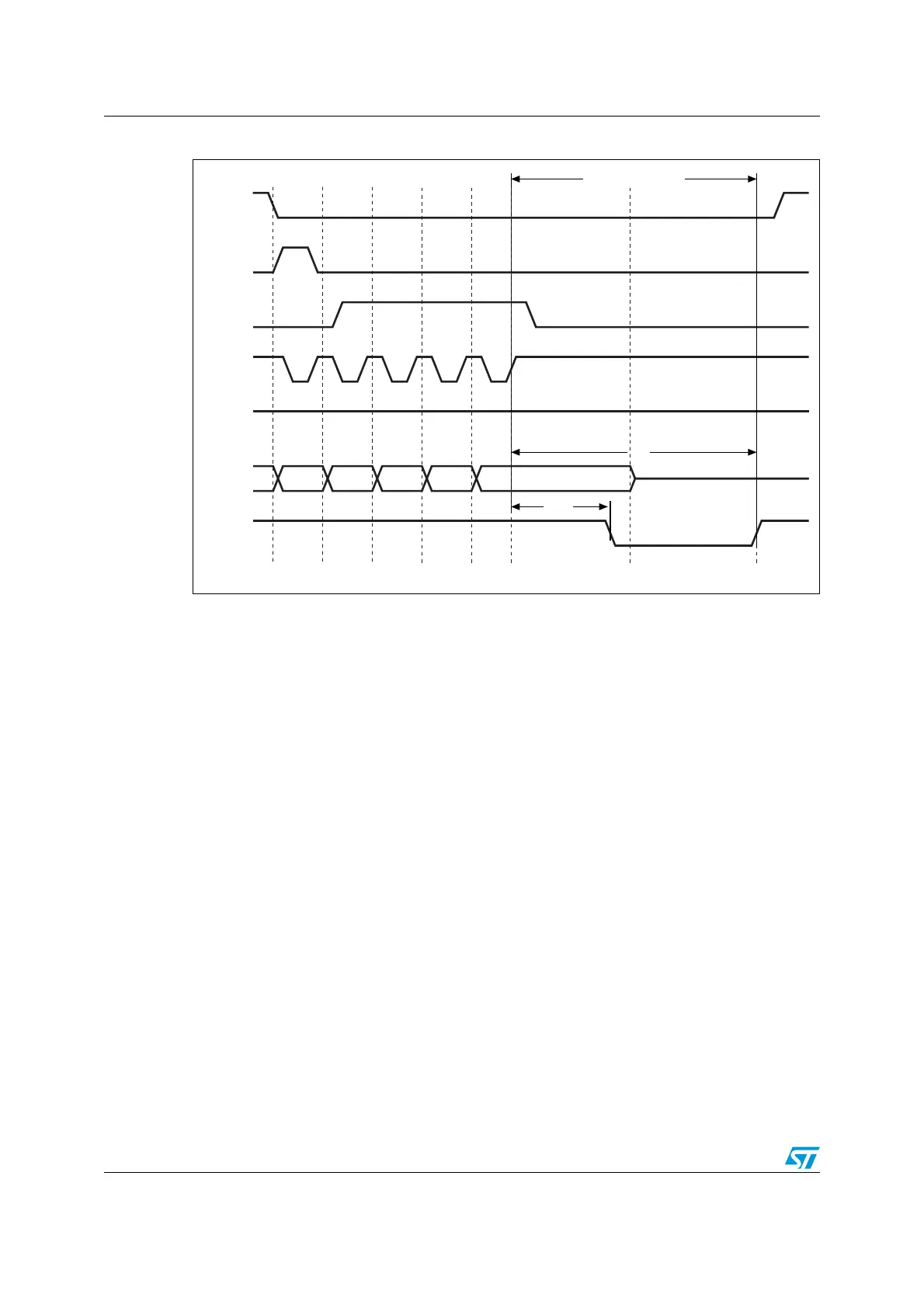
Figure 175. Access to non ‘CE don’t care’ NAND-Flash
1. CPU wrote byte 0x00 at address 0x7001 0000.
2. CPU wrote byte A7~A0 at address 0x7002 0000.
3. CPU wrote byte A16~A9 at address 0x7002 0000.
4. CPU wrote byte A24~A17 at address 0x7002 0000.
5. CPU wrote byte A25 at address 0x7802 0000: FSMC performs a write access using FSMC_PATT2 timing
definition, where ATTHOLD ≥ 7 (providing that (7+1) × HCLK = 112 ns > t
WB
max). This guarantees that
NCE remains low until R/NB goes low and high again (only requested for NAND Flash memories where
NCE is not don’t care).
When this functionality is needed, it can be guaranteed by programming the MEMHOLD
value to meet the t
WB
timing, however any CPU read or write access to the NAND Flash
then has the hold delay of (MEMHOLD + 1) HCLK cycles inserted from the rising edge of
the NWE signal to the next access.
To overcome this timing constraint, the attribute memory space can be used by
programming its timing register with an ATTHOLD value that meets the t
WB
timing, and
leaving the MEMHOLD value at its minimum. Then, the CPU must use the common memory
space for all NAND Flash read and write accesses, except when writing the last address
byte to the NAND Flash device, where the CPU must write to the attribute memory space.
In all cases and for every access, R/NB low holds the FSMC controller with NCE low.
NCE
NOE
I/O[7:0]
R/NB
ai14733
High
tWB
CLE
ALE
0x00 A7-A0 A16-A9 A24-A17 A25
tR
NWE
(1) (2) (3) (4) (5)
NCE must stay low
 Loading...


