RM0008 Flexible static memory controller (FSMC)
371/690
The programmable memory parameters include access timings (see Table 7 0 ) and support
for wrap and wait management (for PSRAM and NOR Flash accessed in burst mode).
18.5.1 External memory interface signals
Tabl e 7 1, Ta bl e 72 and Tabl e 7 3 list the signals that are typically used to interface NOR
Flash and PSRAM.
Note: Prefix “N”. specifies the associated signal as active low.
NOR Flash, nonmultiplexed I/Os
NOR Flash memories are addressed in 16-bit words. The maximum capacity is 512 Mbit (26
address lines).
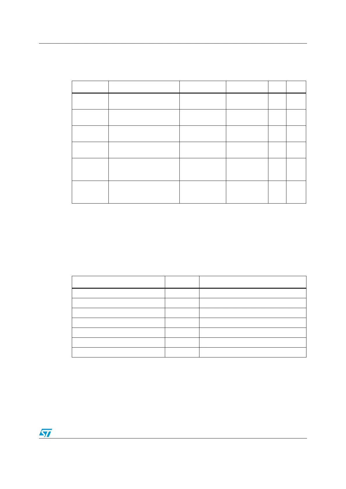
Table 70. Programmable NOR/PSRAM access parameters
Parameter Function Access mode Unit Min. Max.
Address
setup
Duration of the address
setup phase
Asynchronous
AHB clock cycle
(HCLK)
1 16
Address hold
Duration of the address hold
phase
Asynchronous,
muxed I/Os
AHB clock cycle
(HCLK)
1 16
Data setup
Duration of the data setup
phase
Asynchronous
AHB clock cycle
(HCLK)
1 256
Bust turn
Duration of the bus
turnaround phase
Asynchronous and
synchronous read
AHB clock cycle
(HCLK)
1 16
Clock divide
ratio
Number of AHB clock cycles
(HCLK) to build one memory
clock cycle (CLK)
Synchronous
AHB clock cycle
(HCLK)
1 16
Data latency
Number of clock cycles to
issue to the memory before
the first data of the burst
Synchronous
Memory clock
cycle (CLK)
2 17
Table 71. Nonmuxed I/O NOR Flash
FSMC signal name I/O Function
CLK O Clock (for synchronous burst)
A[25:0] O Address bus
D[15:0] I/O Bidirectional data bus
NE[x] O Chip select, x = 1..4
NOE O Output enable
NWE O Write enable
NWAIT I NOR Flash wait input signal to the FSMC
 Loading...


