Flexible static memory controller (FSMC) RM0008
402/690
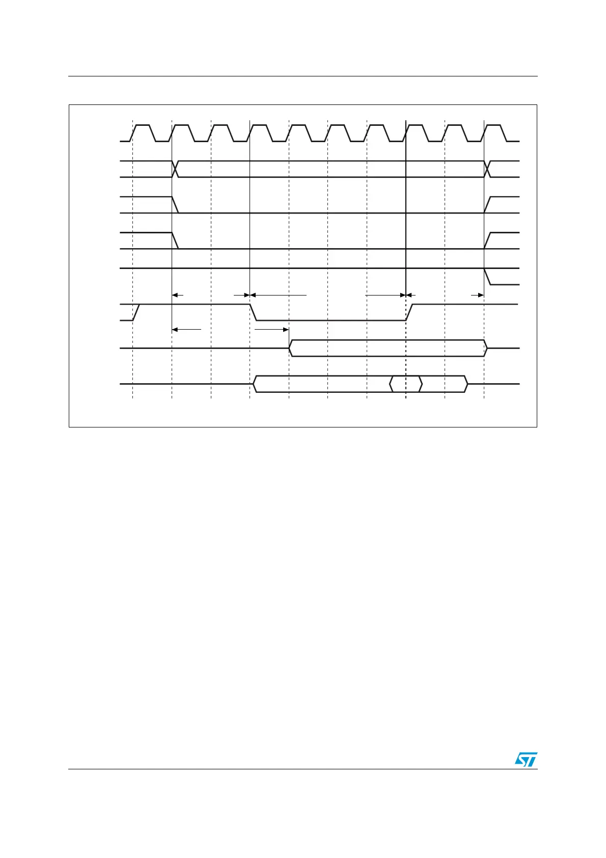
Figure 174. NAND controller timing for common memory access
1. NCE2 remains high (inactive) during the 8-bit access.
2. NOE remains high (inactive) during write access. NWE remains high (inactive) during read access.
NAND Flash operations
As stated previously, the command latch enable (CLE) and address latch enable (ALE)
signals of the NAND Flash device are driven by some address signals of the FSMC
controller. This means that to send a command or an address to the NAND Flash memory,
the CPU has to perform a write to a certain address in its memory space.
A typical page read operation from the NAND Flash device is as follows:
1. Program and enable the corresponding memory bank by configuring the FSMC_PCRx
and FSMC_PMEMx (and for some devices, FSMC_PATTx, see Section 18.6.4: NAND-
Flash ready/busy management on page 403) registers according to the characteristics
of the NAND Flash (PWID bits for the databus width of the NAND Flash, PTYP = 1,
PWAITEN = 1, PBKEN = 1, see section Common memory space timing register 2..4
(FSMC_PMEM2..4) on page 408 for timing configuration).
2. The CPU performs a byte write in the common memory space, with data byte equal to
one Flash command byte (for example 0x00 for Samsung NAND Flash devices). The
CLE input of the NAND Flash is active during the write strobe (low pulse on NWE), thus
the written byte is interpreted as a command by the NAND Flash. Once the command
is latched by the NAND Flash device, it does not need to be written for the following
page read operations.
3. The CPU can send the start address (STARTAD) for a read operation by writing four
bytes (or three for smaller capacity devices), STARTAD[7:0], then STARTAD[16:9],
HCLK
A[25:0]
NCE3
(1)
NCE2
NREG,
NIOW,
NIOR
NWE,
NOE
(2)
write_data
read_data
ai14732
High
Valid
MEMxSET + 1
MEMxWAIT + 1
MEMxHOLD + 1
MEMxHIZ + 1
 Loading...


