RM0008 Flexible static memory controller (FSMC)
399/690
18.6.1 External memory interface signals
The following tables list the signals that are typically used to interface NAND Flash and PC
Card.
Note: Prefix “N”. specifies the associated signal as active low.
8-bit NAND Flash
t
There is no theoretical capacity limitation as the FSMC can manage as many address
cycles as needed.
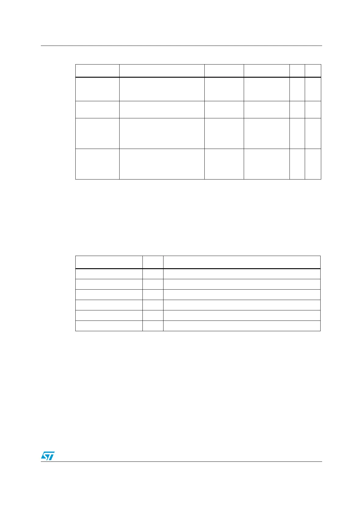
Table 95. Programmable NAND/PC Card access parameters
Parameter Function Access mode Unit Min. Max.
Memory setup
time
Number of clock cycles (HCLK)
to set up the address before the
command assertion
Read/Write
AHB clock cycle
(HCLK)
1 256
Memory wait
Minimum duration (HCLK clock
cycles) of the command assertion
Read/Write
AHB clock cycle
(HCLK)
1 256
Memory hold
Number of clock cycles (HCLK)
to hold the address (and the data
in case of a write access) after
the command de-assertion
Read/Write
AHB clock cycle
(HCLK)
1 255
Memory
databus high-Z
Number of clock cycles (HCLK)
during which the databus is kept
in high-Z state after the start of a
write access
Write
AHB clock cycle
(HCLK)
0 255
Table 96. 8-bit NAND Flash
FSMC signal name I/O Function
A[17] O NAND Flash address latch enable (ALE) signal
A[16] O NAND Flash command latch enable (CLE) signal
D[7:0] I/O 8-bit multiplexed, bidirectional address/data bus
NOE(= NRE) O Output enable (memory signal name: read enable, NRE)
NWE O Write enable
NWAIT I NAND Flash ready/busy input signal to the FSMC
 Loading...


