RM0008 Flexible static memory controller (FSMC)
387/690
18.5.5 Synchronous burst read
The memory clock, CLK, is a submultiple of HCLK according to the value of parameter
CLKDIV.
NOR Flash memories specify a minimum time from NADV assertion to CLK high. To meet
this constraint, the FSMC does not issue the clock to the memory during the first internal
clock cycle of the synchronous access (before NADV assertion). This guarantees that the
rising edge of the memory clock occurs in the middle of the NADV low pulse.
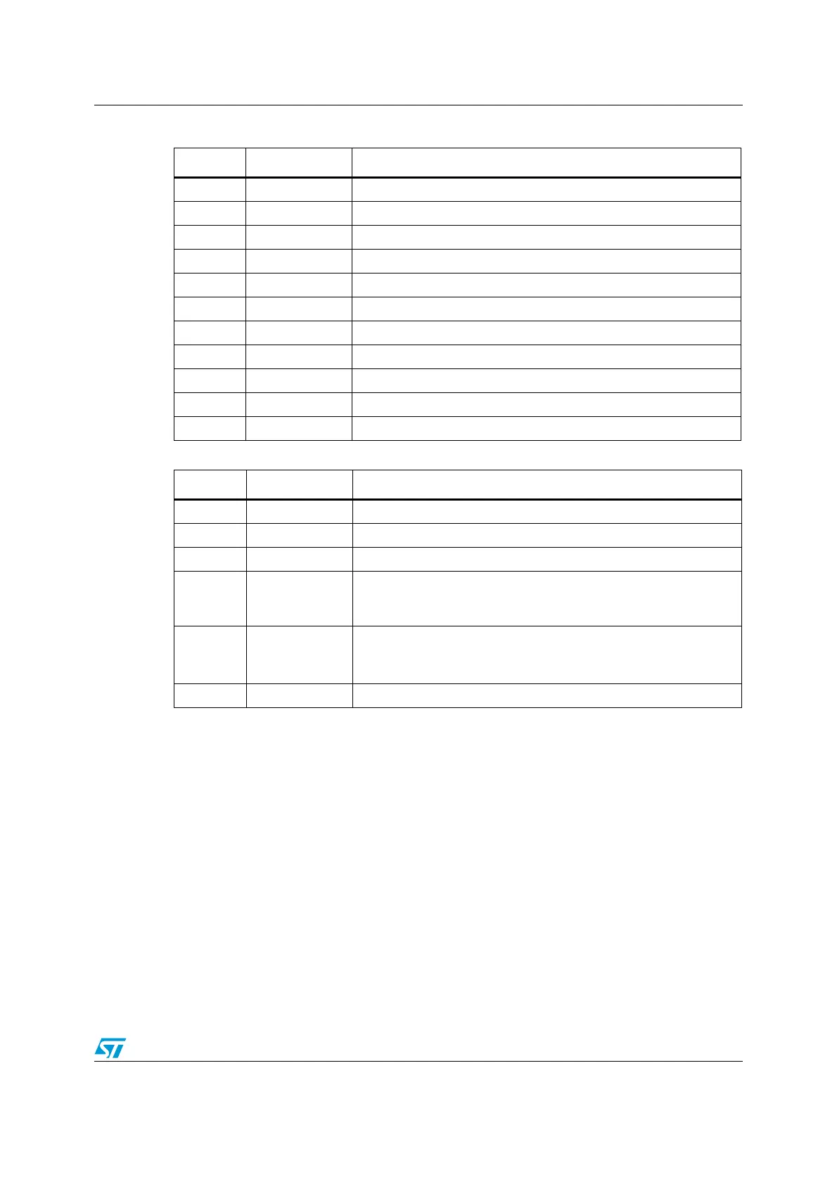
Table 89. FSMC_BCRx bit fields
Bit No. Bit name Value to set
31-15 0x0000
14 EXTMOD 0x0
13-10 0x0
9 WAITPOL Meaningful only if bit 15 is 1.
8 BURSTEN 0x0
7 -
6 FACCEN Set according to memory support
5-4 MWID As needed
3-2 MTYP 10 (NOR)
1 MUXEN 0x1
0 MBKEN 0x1
Table 90. FSMC_TCRx bit fields
Bit No. Bit name Value to set
31-30 0
29-20
19-16 BUSTURN Duration of the last phase of the access (BUSTURN+1 HCLK)
15-8 DATAST
Duration of the second access phase (DATAST+3 HCLK cycles for
read accesses and DATAST+1 HCLK cycles for write accesses).
This value cannot be 0 (minimum is 1)
7-4 ADDHLD
Duration of the middle phase of the access (ADDHLD+1 HCLK
cycles).
This value cannot be 0 (minimum is 1).
3-0 ADDSET Duration of the first access phase (ADDSET+1 HCLK cycles).
 Loading...


