RM0008 Advanced-control timers (TIM1&TIM8)
271/690
12.4.20 DMA address for full transfer (TIMx_DMAR)
Address offset: 0x4C
Reset value: 0x0000
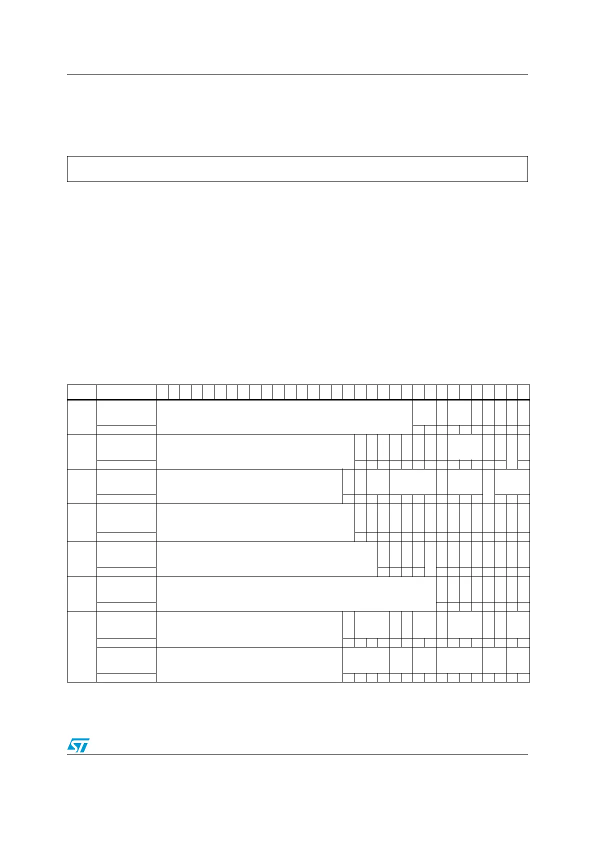
12.4.21 TIM1&TIM8 register map
TIM1&TIM8 registers are mapped as 16-bit addressable registers as described in the table
below:
1514131211109876543210
DMAB[15:0]
rw rw rw rw rw rw rw rw rw rw rw rw rw rw rw rw
Bits 15:0 DMAB[15:0]: DMA register for burst accesses.
A read or write access to the DMAR register accesses the register located at the address:
“(TIMx_CR1 address) + DBA + (DMA index)” in which:
TIMx_CR1 address is the address of the control register 1,
DBA is the DMA base address configured in TIMx_DCR register,
DMA index is the offset automatically controlled by the DMA transfer, depending on the length of the
transfer DBL in the TIMx_DCR register.
Table 56. TIM1&TIM8 Register map and reset values
Offset Register
31
30
29
28
27
26
25
24
23
22
21
20
19
18
17
16
15
14
13
12
11
10
9
8
7
6
5
4
3
2
1
0
0x00
TIMx_CR1
Reserved
CKD
[1:0]
ARPE
CMS
[1:0]
DIR
OPM
URS
UDIS
CEN
Reset value 0000000000
0x04
TIMx_CR2
Reserved
OIS4
OIS3N
OIS3
OIS2N
OIS2
OIS1N
OIS1
TI1S
MMS[2:0]
CCDS
CCUS
Reserved
CCPC
Reset value 0000000000000 0
0x08
TIMx_SMCR
Reserved
ETP
ECE
ETPS
[1:0]
ETF[3:0]
MSM
TS[2:0]
Reserved
SMS[2:0]
Reset value 000000000000 000
0x0C
TIMx_DIER
Reserved
TDE
COMDE
CC4DE
CC3DE
CC2DE
CC1DE
UDE
BIE
TIE
COMIE
CC4IE
CC3IE
CC2IE
CC1IE
UIE
Reset value 000000000000000
0x10
TIMx_SR
Reserved
CC4OF
CC3OF
CC2OF
CC1OF
Reserved
BIF
TIF
COMIF
CC4IF
CC3IF
CC2IF
CC1IF
UIF
Reset value 0000 00000000
0x14
TIMx_EGR
Reserved
BG
TG
COM
CC4G
CC3G
CC2G
CC1G
UG
Reset value 00000000
0x18
TIMx_CCMR1
Output Compare
mode
Reserved
OC2CE
OC2M
[2:0]
OC2PE
OC2FE
CC2S
[1:0]
OC1CE
OC1M
[2:0]
OC1PE
OC1FE
CC1S
[1:0]
Reset value 0000000000000000
TIMx_CCMR1
Input Capture
mode
Reserved
IC2F[3:0]
IC2
PSC
[1:0]
CC2S
[1:0]
IC1F[3:0]
IC1
PSC
[1:0]
CC1S
[1:0]
Reset value 0000000000000000
 Loading...


