RM0008 Flexible static memory controller (FSMC)
401/690
18.6.3 Timing diagrams for NAND, ATA and PC Card
Each CompactFlash and NAND Flash memory bank is managed through a set of registers:
● Control register: FSMC_PCRx
● Interrupt status register: FSMC_SRx
● ECC register: FSMC_ECCRx
● Timing register for Common memory space: FSMC_PMEMx
● Timing register for Attribute memory space: FSMC_PATTx
● Timing register for I/O space: FSMC_PIOx
Each timing configuration register contains three parameters used to define number of
HCLK cycles for the three phases of any CompactFlash or NAND Flash access, plus one
parameter that defines the timing for starting driving the databus in the case of a write.
Figure 174 shows the timing parameter definitions for common memory accesses, knowing
that Attribute and I/O (only for PC Card) memory space access timings are similar.
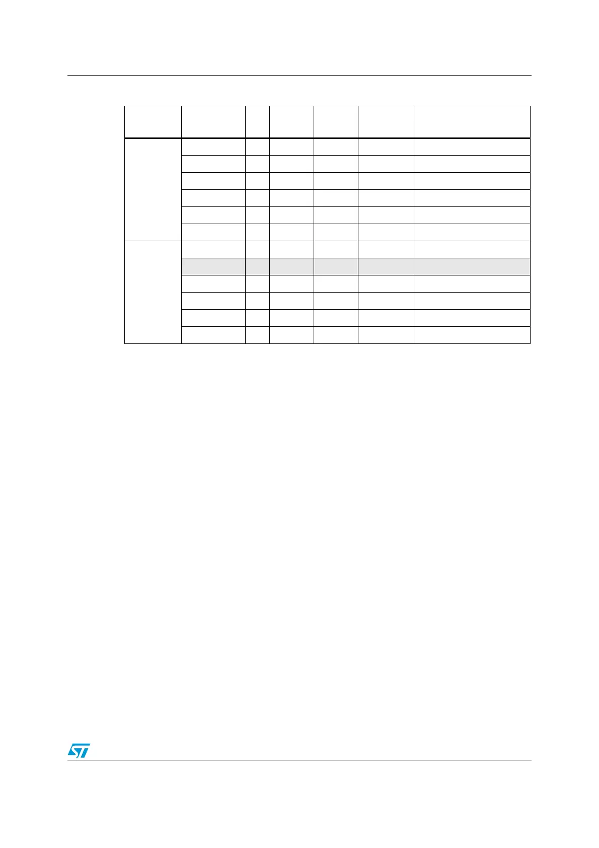
Table 99. Supported memories and transactions
Device Mode R/W
AHB
data size
Memory
data size
Allowed/
not allowed
Comments
NAND 8-bit
Asynchronous R 8 8 Y
Asynchronous W 8 8 Y
Asynchronous R 16 8 Y Split into 2 FSMC accesses
Asynchronous W 16 8 Y Split into 2 FSMC accesses
Asynchronous R 32 8 Y Split into 4 FSMC accesses
Asynchronous W 32 8 Y Split into 4 FSMC accesses
NAND 16-bit
Asynchronous R 8 16 Y
Asynchronous W 8 16 N
Asynchronous R 16 16 Y
Asynchronous W 16 16 Y
Asynchronous R 32 16 Y Split into 2 FSMC accesses
Asynchronous W 32 16 Y Split into 2 FSMC accesses
 Loading...


