Memory and bus architecture RM0008
36/690
2.3.1 Peripheral memory map
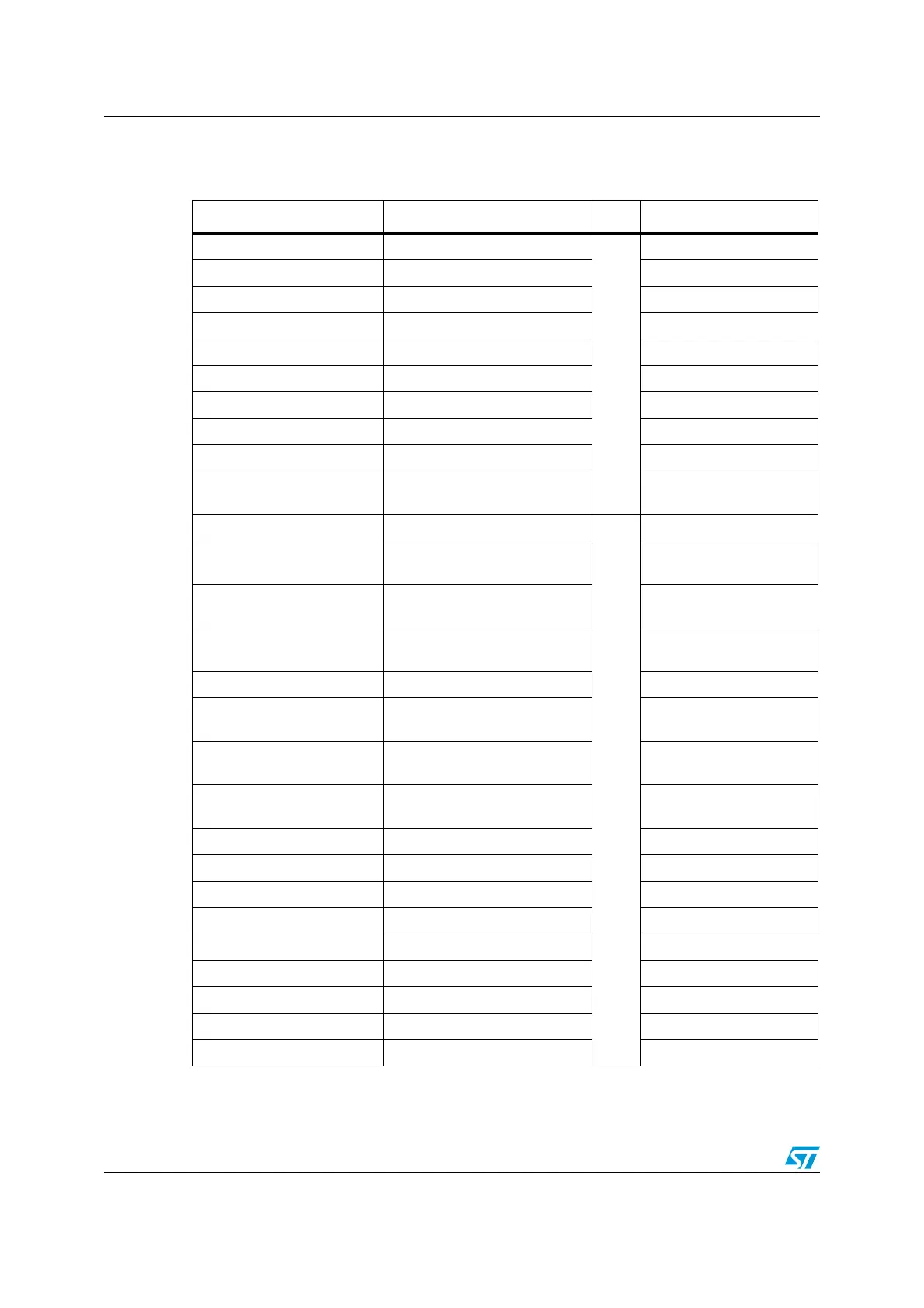
Table 1. Register boundary addresses
Boundary address Peripheral Bus Register map
0x4002 2400 - 0x4002 3FFF Reserved
AHB
0x4002 3000 - 0x4002 33FF CRC Section 3.4.4 on page 47
0x4002 2000 - 0x4002 23FF Flash memory interface
0x4002 1400 - 0x4002 1FFF Reserved
0x4002 1000 - 0x4002 13FF Reset and Clock control RCC Section 6.3.11 on page 96
0x4002 0800 - 0x4002 0FFF Reserved
0x4002 0400 - 0x4002 07FF DMA2 Section 9.4.7 on page 146
0x4002 0000 - 0x4002 03FF DMA1 Section 9.4.7 on page 146
0x4001 8400 - 0x4001 7FFF Reserved
0x4001 8000 - 0x4001 83FF SDIO
Section 19.9.16 on page
466
0x4001 4000 - 0x4001 7FFF Reserved
APB2
0x4001 3C00 - 0x4001 3FFF ADC3
Section 10.12.15 on page
182
0x4001 3800 - 0x4001 3BFF USART1
Section 24.6.8 on page
649
0x4001 3400 - 0x4001 37FF TIM8 timer
Section 12.4.21 on page
271
0x4001 3000 - 0x4001 33FF SPI1 Section 22.5 on page 569
0x4001 2C00 - 0x4001 2FFF TIM1 timer
Section 12.4.21 on page
271
0x4001 2800 - 0x4001 2BFF ADC2
Section 10.12.15 on page
182
0x4001 2400 - 0x4001 27FF ADC1
Section 10.12.15 on page
182
0x4001 2000 - 0x4001 23FF GPIO Port G Section 7.5 on page 121
0x4001 1C00 - 0x4001 1FFF GPIO Port F Section 7.5 on page 121
0x4001 1800 - 0x4001 1BFF GPIO Port E Section 7.5 on page 121
0x4001 1400 - 0x4001 17FF GPIO Port D Section 7.5 on page 121
0x4001 1000 - 0x4001 13FF GPIO Port C Section 7.5 on page 121
0x4001 0C00 - 0x4001 0FFF GPIO Port B Section 7.5 on page 121
0x4001 0800 - 0x4001 0BFF GPIO Port A Section 7.5 on page 121
0x4001 0400 - 0x4001 07FF EXTI Section 8.3.7 on page 133
0x4001 0000 - 0x4001 03FF AFIO Section 7.5 on page 121
 Loading...


