RM0008 Flexible static memory controller (FSMC)
369/690
HADDR[25:0] contain the external memory address. Since HADDR is a byte address
whereas the memory is addressed in words, the address actually issued to the memory
varies according to the memory data width, as shown in the following table.
Wrap support for NOR Flash/PSRAM
Each NOR Flash/PSRAM memory bank can be configured to support wrap accesses.
On the memory side, two cases must be considered depending on the access mode:
asynchronous or synchronous.
● Asynchronous mode: in this case, wrap accesses are fully supported as long as the
address is supplied for every single access.
● Synchronous mode: in this case, the FSMC issues the address only once, and then
the burst transfer is sequenced by the FSMC clock CLK.
Some NOR memories support linear burst with wrap-around accesses, in which a fixed
number of words is read from consecutive addresses modulo N (N is typically 8, 16 or
32 and can be programmed through the NOR Flash configuration register). In this case,
it is possible to set the memory wrap mode identical to the AHB master wrap mode.
Otherwise, in the case when the memory wrap mode and the AHB master wrap mode
cannot be set identically, wrapping should be disabled (through the appropriate bit in the
FSMC configuration register) and the wrap transaction split into two consecutive linear
transactions.
18.4.2 NAND/PC Card address mapping
In this case, three banks are available, each of them divided into memory spaces as
indicated in Ta ble 6 8.
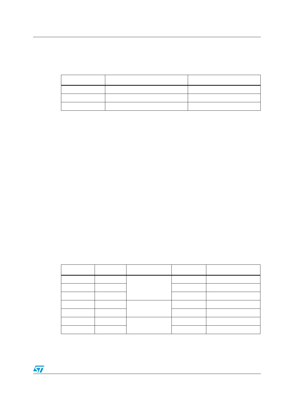
Table 67. External memory address
Memory width Data address issued to the memory Maximum memory capacity (bits)
8-bit HADDR[25:0] 64 Mbytes x 8 = 512 Mbit
16-bit HADDR[25:1] >> 1 64 Mbytes/2 x 16 = 512 Mbit
32-bit HADDR[25:2] >>2 64 Mbytes/4 x 32 = 512 Mbit
Table 68. Memory mapping and timing registers
Start address End address FSMC Bank Memory space Timing register
0x9C00 0000 0x9FFF FFFF
Bank 4 - PC card
I/O FSMC_PIO4 (0xB0)
0x9800 0000 0x9BFF FFFF Attribute FSMC_PATT4 (0xAC)
0x9000 0000 0x93FF FFFF Common FSMC_PMEM4 (0xA8)
0x8800 0000 0x8BFF FFFF
Bank 3 - NAND Flash
Attribute FSMC_PATT3 (0x8C)
0x8000 0000 0x83FF FFFF Common FSMC_PMEM3 (0x88)
0x7800 0000 0x7BFF FFFF
Bank 2- NAND Flash
Attribute FSMC_PATT2 (0x6C)
0x7000 0000 0x73FF FFFF Common FSMC_PMEM2 (0x68)
 Loading...


