Inter-integrated circuit (I
2
C) interface RM0008
584/690
Header matched (10-bit mode only): the interface generates an acknowledge pulse if the
ACK bit is set and waits for the 8-bit slave address.
Address matched: the interface generates in sequence:
● An acknowledge pulse if the ACK bit is set
● The ADDR bit is set by hardware and an interrupt is generated if the ITEVFEN bit is
set.
● If ENDUAL=1, the software has to read the DUALF bit to check which slave address
has been acknowledged.
In 10-bit mode, after receiving the address sequence the slave is always in Receiver mode.
It will enter Transmitter mode on receiving a repeated Start condition followed by the header
sequence with matching address bits and the least significant bit set (11110xx1).
The TRA bit indicates whether the slave is in Receiver or Transmitter mode.
Slave transmitter
Following the address reception and after clearing ADDR, the slave sends bytes from the
DR register to the SDA line via the internal shift register.
The slave stretches SCL low until ADDR is cleared and DR filled with the data to be sent
(see Figure 232 Transfer sequencing EV1 EV3).
When the acknowledge pulse is received:
● The TxE bit is set by hardware with an interrupt if the ITEVFEN and the ITBUFEN bits
are set.
If TxE is set and a data was not written in the DR register before the end of the last data
transmission, the BTF bit is set and the interface waits for a write in the DR register,
stretching SCL low.
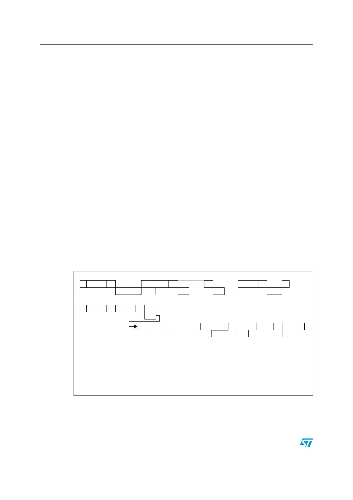
Figure 232. Transfer sequence diagram for slave transmitter
7-bit slave transmitter:
10-bit slave transmitter
Legend: S= Start, S
r
= Repeated Start, P= Stop, A= Acknowledge, NA= Non-acknowledge,
EVx= Event (with interrupt if ITEVFEN=1)
EV1: ADDR=1, cleared by reading SR1 followed by reading SR2
EV3-1: TxE=1, shift register empty.
EV3: TxE=1, cleared by writing DR; shift register not empty
EV3-2: AF=1; AF is cleared by writing ‘0’ in AF bit of SR1 register.
S Address A Data1 A Data2 A
.....
DataN NA P
EV1 EV3-1 EV3 EV3 EV3 EV3-2
S Header A Address A
EV1
S
r
Header A Data1 A
....
.
DataN NA P
EV1 EV3_1 EV3 EV3 EV3-2
 Loading...


