RM0008 Inter-integrated circuit (I
2
C) interface
589/690
After the Stop condition generation, the interface goes automatically back to slave mode
(M/SL bit cleared).
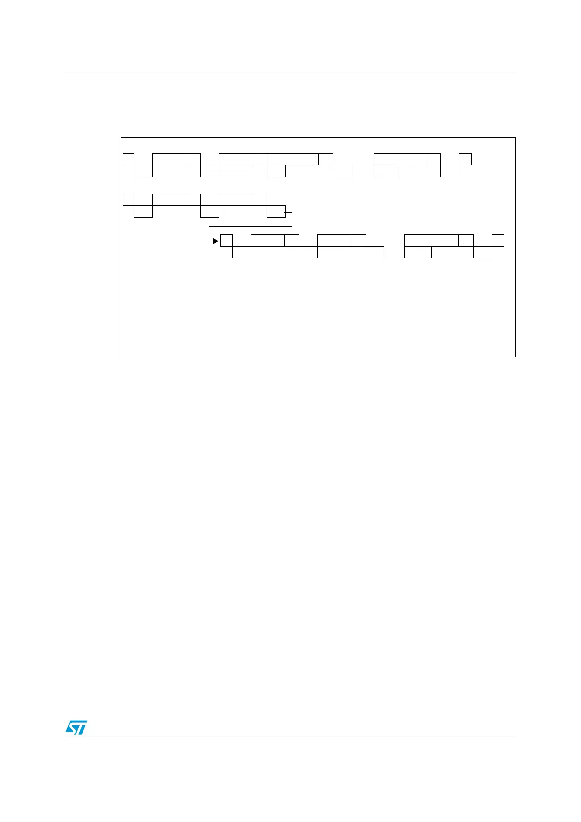
Figure 235. Transfer sequence diagram for master receiver
23.3.4 Error conditions
The following are the error conditions which may cause communication to fail.
Bus error (BERR)
This error occurs when the I
2
C interface detects a Stop or a Start condition during a byte
transfer. In this case,
● The BERR bit is set and an interrupt is generated if the ITERREN bit is set
● In case of Slave: data is discarded and the lines are released by hardware:
– in case of misplaced start, the slave considers it is a restart and waits for address,
or stop condition.
– in case of misplaced stop, the slave reacts like for a stop condition and the lines
are released by hardware.
Acknowledge failure (AF)
This error occurs when the interface detects a non-acknowledge bit. In this case,
● The AF bit is set and an interrupt is generated if the ITERREN bit is set
● A transmitter which receives a NACK must reset the communication:
– If Slave: lines are released by hardware
– If Master: a Stop condition must be generated by software
7-bit Master Receiver:
10-bit Master Receiver
Legend: S= Start, S
r
= Repeated Start, P= Stop, A= Acknowledge, NA= Non-acknowledge,
EVx= Event (with interrupt if ITEVFEN=1)
EV5: SB=1, cleared by reading SR1 register followed by writing DR register.
EV6: ADDR=1, cleared by reading SR1 register followed by reading SR2. In 10-bit master receiver mode, this se-
quence should be followed by writing CR2 with START = 1.
EV7: RxNE=1 cleared by reading DR register.
EV7_1: RxNE=1 cleared by reading DR register, program ACK=0 and STOP request
EV9: ADD10=1, cleared by reading SR1 register followed by writing DR register.
S Address A Data1 A Data2 A
.....
DataN NA P
EV5 EV6 EV7 EV7 EV7_1 EV7
S Header A Address A
EV5 EV9 EV6
S
r
Header A Data1 A
.....
DataN NA P
EV5 EV6 EV7 EV7_1 EV7
 Loading...


