General-purpose timer (TIMx) RM0008
328/690
13.4.18 DMA address for full transfer (TIMx_DMAR)
Address offset: 0x4C
Reset value: 0x0000
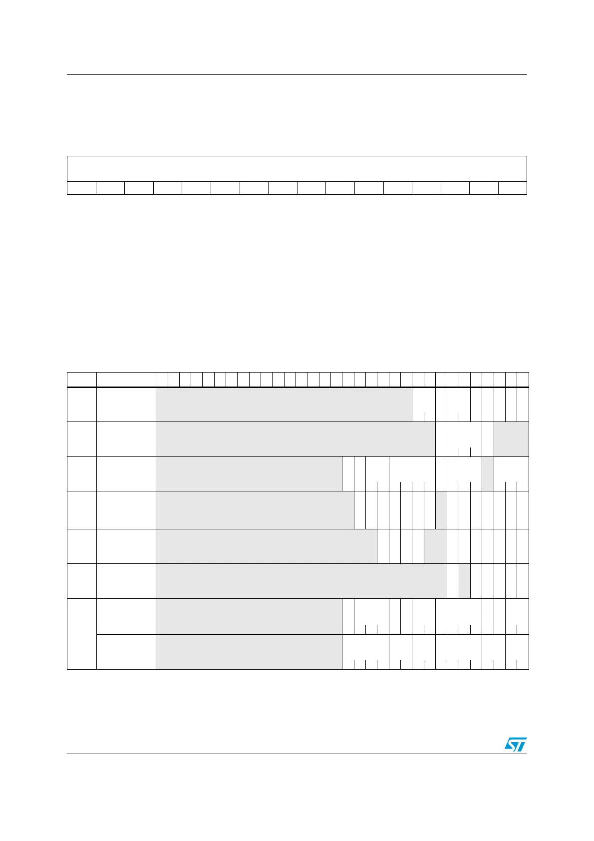
13.4.19 TIMx register map
TIMx registers are mapped as 16-bit addressable registers as described in the table below:
1514131211109876543210
DMAB[15:0]
rw rw rw rw rw rw rw rw rw rw rw rw rw rw rw rw
Bits 15:0 DMAB[15:0]: DMA register for burst accesses.
A read or write access to the DMAR register accesses the register located at the address:
“(TIMx_CR1 address) + DBA + (DMA index)” in which:
TIMx_CR1 address is the address of the control register 1,
DBA is the DMA base address configured in the TIMx_DCR register,
DMA index is the offset automatically controlled by the DMA transfer, depending on the length of the
transfer DBL in the TIMx_DCR register.
Table 60. TIMx register map and reset values
Offset Register
31
30
29
28
27
26
25
24
23
22
21
20
19
18
17
16
15
14
13
12
11
10
9
8
7
6
5
4
3
2
1
0
0x00
TIMx_CR1
Reserved
CKD
[1:0]
ARPE
CMS
[1:0]
DIR
OPM
URS
UDIS
CEN
Reset value 0000000000
0x04
TIMx_CR2
Reserved
TI1S
MMS[2:0]
CCDS
Reserved
Reset value 00000
0x08
TIMx_SMCR
Reserved
ETP
ECE
ETPS
[1:0]
ETF[3:0]
MSM
TS[2:0]
Reserved
SMS[2:0]
Reset value 000000000000 000
0x0C
TIMx_DIER
Reserved
TDE
COMDE
CC4DE
CC3DE
CC2DE
CC1DE
UDE
Reserved
TIE
COMIE
CC4IE
CC3IE
CC2IE
CC1IE
UIE
Reset value 0
000000 00
00000
0x10
TIMx_SR
Reserved
CC4OF
CC3OF
CC2OF
CC1OF
Reserved
TIF
COMIF
CC4IF
CC3IF
CC2IF
CC1IF
UIF
Reset value 0000 0000000
0x14
TIMx_EGR
Reserved
TG
Reserved
CC4G
CC3G
CC2G
CC1G
UG
Reset value 0 00000
0x18
TIMx_CCMR1
Output Compare
mode
Reserved
OC2CE
OC2M
[2:0]
OC2PE
OC2FE
CC2S
[1:0]
OC1CE
OC1M
[2:0]
OC1PE
OC1FE
CC1S
[1:0]
Reset value 0000000000000000
TIMx_CCMR1
Input Capture
mode
Reserved
IC2F[3:0]
IC2
PSC
[1:0]
CC2S
[1:0]
IC1F[3:0]
IC1
PSC
[1:0]
CC1S
[1:0]
Reset value 0000000000000000
 Loading...


