Embedded Flash memory (FLASH) RM0351
108/1830 DocID024597 Rev 5
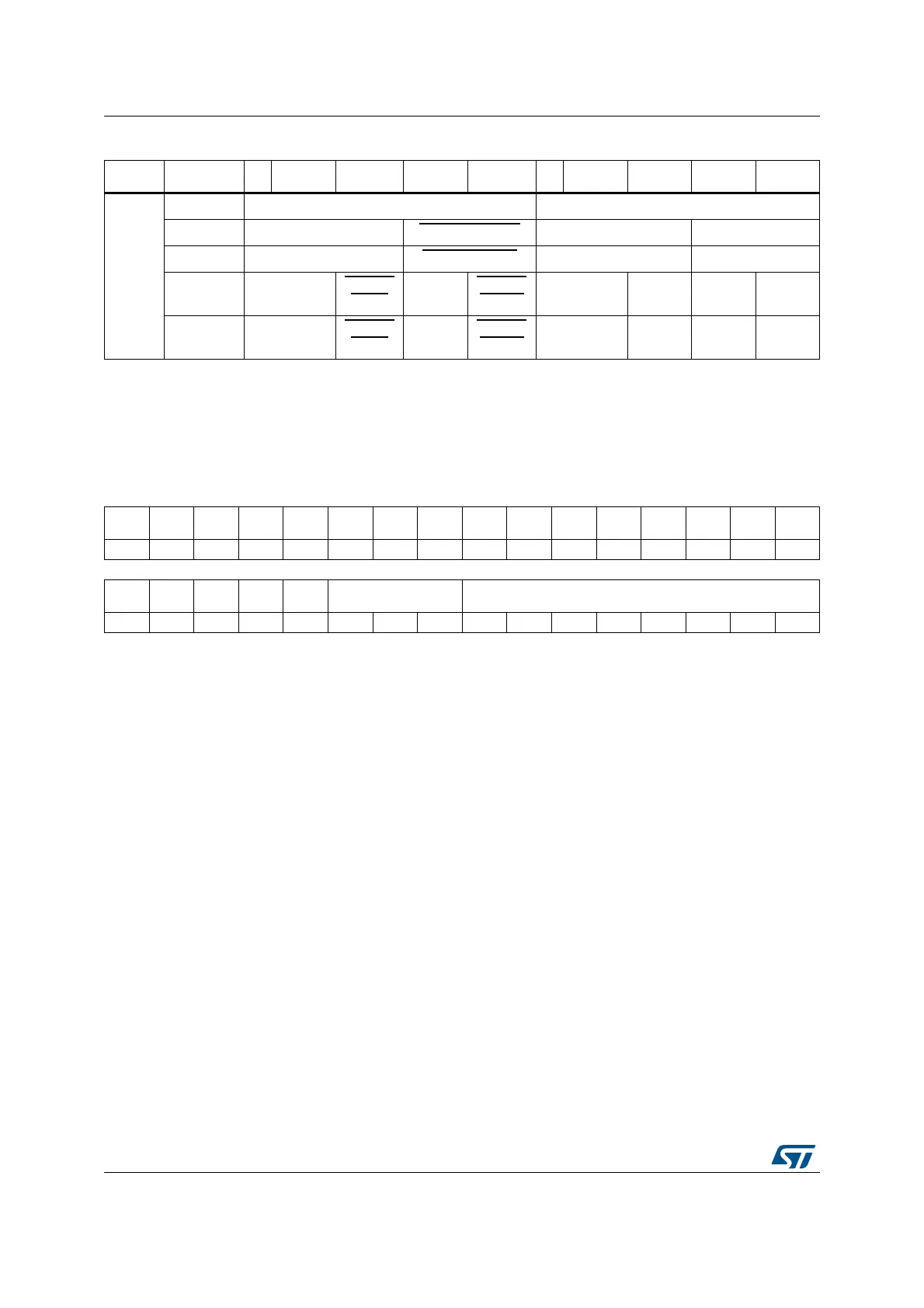
User and read protection option bytes
Flash memory address: 0x1FFF 7800
ST production value: 0xFFEF F8AA
Bank 2
1FFFF800 Unused Unused
1FFFF808 Unused PCROP2_STRT
Unused PCROP2_STRT
1FFFF810 Unused PCROP2_END
Unused PCROP2_END
1FFFF818 Unused
WRP2A
_END
Unused
WRP2A
_STRT
Unused
WRP2A
_END
Unused
WRP2A
_STRT
1FFFF820 Unused
WRP2B
_END
Unused
WRP2B
_STRT
Unused
WRP2B
_END
Unused
WRP2B
_STRT
Table 13. Option byte organization (continued)
BANK Address 63 [62:56] [55:48] [47:40] [39:32] 31 [30:24] [23:16] [15:8] [7:0]
31 30 29 28 27 26 25 24 23 22 21 20 19 18 17 16
Res. Res. Res. Res.
n
BOOT0
nSW
BOOT0
SRAM2
_RST
SRAM2
_PE
n
BOOT1
Res.
DUAL
BANK
BFB2
WWDG
_SW
IWGD_
STDBY
IWDG_
StOP
IWDG_
SW
rrrrr rrrrrr
1514131211109876543210
Res.
nRST_
SHDW
nRST_
STDBY
nRST_
STOP
Res. BOR_LEV[2:0] RDP[7:0]
rrr rrrrrrrrrrr
Bits 31:28 Not used
Bit 27 nBOOT0: nBOOT0 option bit (only for STM32L496/4A6 devices)
0: nBOOT0 = 0
1: nBOOT0 = 1
Bit 26 nSWBOOT0: Software BOOT0 (only for STM32L496/4A6 devices)
0: BOOT0 taken from the option bit nBOOT0
1: BOOT0 taken from PH3/BOOT0 pin
Bit 25 SRAM2_RST: SRAM2 Erase when system reset
0: SRAM2 erased when a system reset occurs
1: SRAM2 is not erased when a system reset occurs
Bit 24 SRAM2_PE: SRAM2 parity check enable
0: SRAM2 parity check enable
1: SRAM2 parity check disable
Bit 23 nBOOT1: Boot configuration
Together with the BOOT0 pin, this bit selects boot mode from the Flash main
memory, SRAM1 or the System memory. Refer to Section 2.6: Boot
configuration.
Bit 22 Not used
 Loading...


