Inter-integrated circuit (I2C) interface RM0351
1288/1830 DocID024597 Rev 5
39.7.2 Control register 2 (I2C_CR2)
Address offset: 0x04
Reset value: 0x0000 0000
Access: No wait states, except if a write access occurs while a write access to this register is
ongoing. In this case, wait states are inserted in the second write access until the previous
one is completed. The latency of the second write access can be up to 2 x PCLK1 + 6 x
I2CCLK.
Bit 2 RXIE: RX Interrupt enable
0: Receive (RXNE) interrupt disabled
1: Receive (RXNE) interrupt enabled
Bit 1 TXIE: TX Interrupt enable
0: Transmit (TXIS) interrupt disabled
1: Transmit (TXIS) interrupt enabled
Bit 0 PE: Peripheral enable
0: Peripheral disable
1: Peripheral enable
Note: When PE=0, the I2C SCL and SDA lines are released. Internal state machines and
status bits are put back to their reset value. When cleared, PE must be kept low for at
least 3 APB clock cycles.
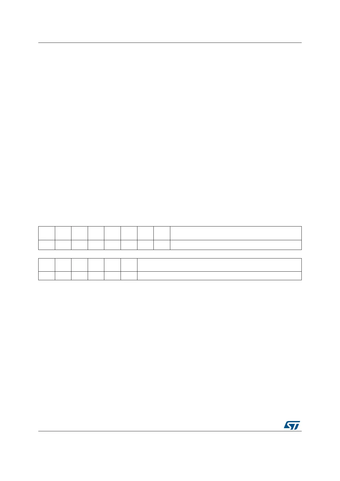
31 30 29 28 27 26 25 24 23 22 21 20 19 18 17 16
Res. Res. Res. Res. Res.
PEC
BYTE
AUTO
END
RE
LOAD
NBYTES[7:0]
rs rw rw rw
1514131211109876543210
NACK STOP START
HEAD
10R
ADD10
RD_
WRN
SADD[9:0]
rs rs rs rw rw rw rw
 Loading...


