DocID024597 Rev 5 779/1830
RM0351 Liquid crystal display controller (LCD)
787
1. Configure and enable the LCD IRQ channel in the NVIC
2. Configure the LCD to generate interrupts
25.6 LCD registers
The peripheral registers have to be accessed by words (32-bit).
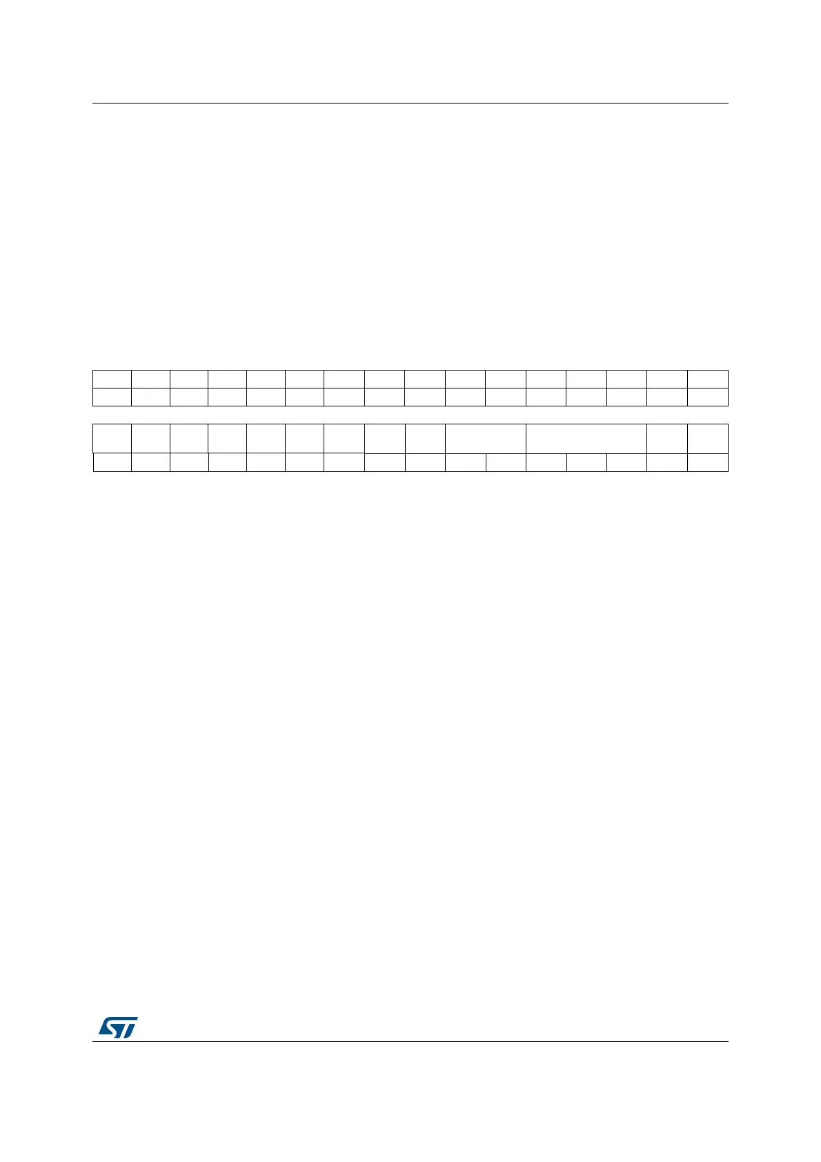
25.6.1 LCD control register (LCD_CR)
Address offset: 0x00
Reset value: 0x0000 0000
31 30 29 28 27 26 25 24 23 22 21 20 19 18 17 16
Res. Res. Res. Res. Res. Res. Res. Res. Res. Res. Res. Res. Res. Res. Res. Res.
1514131211109876543210
Res. Res. Res. Res. Res. Res. Res. BUFEN
MUX_
SEG
BIAS[1:0] DUTY[2:0] VSEL LCDEN
rw rw rw rw rw rw rw rw rw
Bits 31:9 Reserved, must be kept at reset value
Bit 8 BUFEN: Voltage output buffer enable
This bit is used to enable/disable the voltage output buffer for higher driving capability.
0: Output buffer disabled
1: Output buffer enabled
Bit 7 MUX_SEG: Mux segment enable
This bit is used to enable SEG pin remapping. Four SEG pins can be multiplexed with
SEG[31:28]. See Section 25.3.7.
0: SEG pin multiplexing disabled
1: SEG[31:28] are multiplexed with SEG[43:40]
Bits 6:5 BIAS[1:0]: Bias selector
These bits determine the bias used. Value 11 is forbidden.
00: Bias 1/4
01: Bias 1/2
10: Bias 1/3
11: Reserved
 Loading...


