RTC6 boards
Doc. Rev. 1.0.21 en-US
4 RTC6 PCIe Board – Layout and Interfaces
85
For data output using the McBSP interface, see
Chapter 9.1.7 ”McBSP Interface”, page 287.
For data input using the McBSP interface, see
Chapter 9.2.4 ”McBSP Interface”, page 288.
mcbsp_init allows setting a data delay for the McBSP
data transmission independently for the transmitter
and receiver. Possible values range from 0 to 2
(Default: 1).
All signals are referenced to GND
(1)
.
RTC6 PCIe Board as Transmitter
The following specifications apply to CLKX0, FSX0
and DX0:
• Signal level 3.3 V TTL
• McBSP mode:
– Single phase frame
– Single element per frame
– 32 bits per element
– Data delay
XDelay
bits
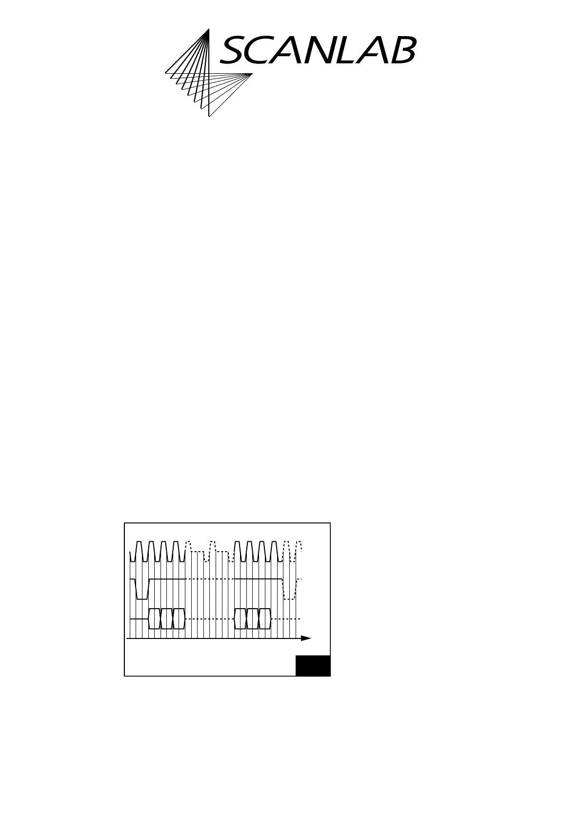
• The timing diagram of the McBSP signals is
shown in Figure 29. A frame synchronization
signal (active-LOW) is generated upon the rising
edge of the clock and held for one clock cycle
(1 data bit). The 32 data bits are transmitted after
XDelay
clock cycles at the rising edges of the clock
and in the sequence Bit #31…Bit #0. The
transmission frequency is by default 8 MHz (4 µs
per data word). Alternatively, a value between
4 MHz and 16 MHz can be set by
set_mcbsp_freq.
RTC6 PCIe Board as Receiver
The following specifications apply to CLKR0, FSR0,
DR0:
• Signal level 3.3 V or 5 V TTL.
• McBSP mode:
– Single phase frame
– Single element per frame
– 32 bits per element
– Data delay
RDelay
bits
The timing diagram of the McBSP signals is shown in
Figure 29. The frame synchronization signal
(active-LOW) generated upon a rising edge (of an
external clock signal) is detected upon the clock’s
next falling edge (trailing edge of the external clock
pulse). The duration of the frame synchronization
signal is irrelevant. After
RDelay
clock cycles the 32
data bits are detected with each additional falling
edge of the clock signals in the sequence
Bit #31…Bit #0, provided they are transmitted with
rising edges.
When doing so, observe the following Notes:
– The McBSP interface always ignores the first
frame synchronization signal after a
load_program_file or mcbsp_init. Therefore,
the data provided is not transmitted. If
necessary, a dummy value should be initially
sent to the interface. You can use read_mcbsp
to check for successful transmission.
– The bit frequency (receiving frequency) is
exclusively determined by the incoming clock
pulses and has a maximum limit of 16 MHz.
– The last data bit (Bit #0) must be followed by
transmission of at least one additional external
clock cycle to ensure that the interface’s DSP
side acquires and buffers the data word.
Simultaneously with this clock cycle, you can
already initiate another new transfer by a frame
synchronization signal.
(1) See footnote on page 73.
29
Timing diagram of McBSP signals at 1 bit data delay.
Default:
XDelay
=
RDelay
= 1.
t
DX/R
CLKX/R
FSX/R
B31 B30 B29 B2 B1 B0