RM0440 Rev 4 1115/2126
RM0440 Advanced-control timers (TIM1/TIM8/TIM20)
1226
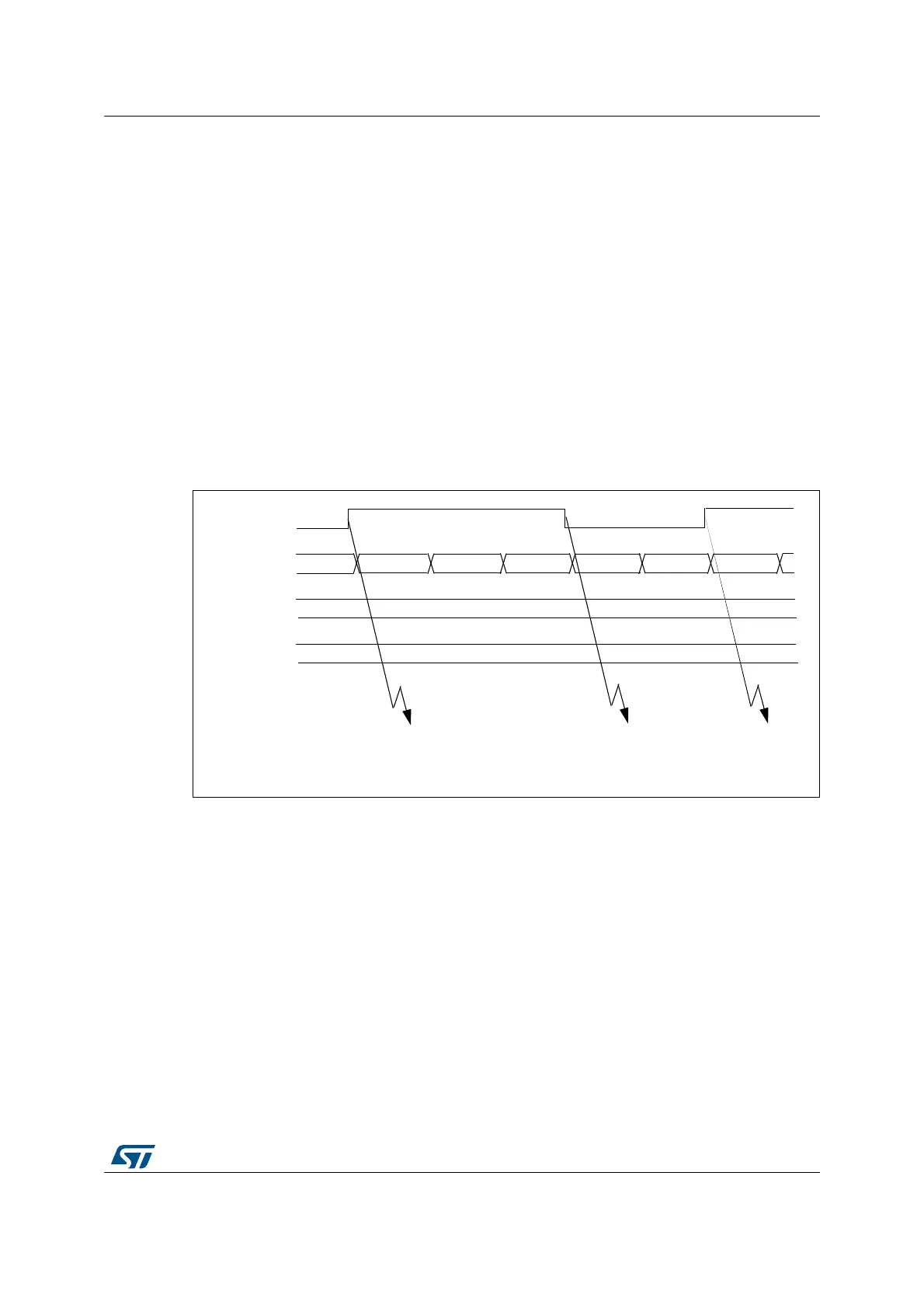
The period and the pulsewidth of a PWM signal applied on tim_ti1 can be measured using
the following procedure:
• Select the active input for TIMx_CCR1: write the CC1S bits to 01 in the TIMx_CCMR1
register (tim_ti1 selected).
• Select the active polarity for tim_ti1fp1 (used both for capture in TIMx_CCR1 and
counter clear): write the CC1P and CC1NP bits to ‘0’ (active on rising edge).
• Select the active input for TIMx_CCR2: write the CC2S bits to 10 in the TIMx_CCMR1
register (tim_ti1 selected).
• Select the active polarity for tim_ti1fp2 (used for capture in TIMx_CCR2): write the
CC2P and CC2NP bits to CC2P/CC2NP=’10’ (active on falling edge).
• Select the valid trigger input: write the TS bits to 00101 in the TIMx_SMCR register
(tim_ti1fp1 selected).
• Configure the slave mode controller in reset mode: write the SMS bits to 0100 in the
TIMx_SMCR register.
• Enable the captures: write the CC1E and CC2E bits to ‘1’ in the TIMx_CCER register.
Figure 300. PWM input mode timing
28.3.11 Forced output mode
In output mode (CCxS bits = 00 in the TIMx_CCMRx register), each output compare signal
(tim_ocxref and then tim_ocx/tim_ocxn) can be forced to active or inactive level directly by
software, independently of any comparison between the output compare register and the
counter.
To force an output compare signal (tim_ocxref/tim_ocx) to its active level, user just needs to
write 0101 in the OCxM bits in the corresponding TIMx_CCMRx register. Thus tim_ocxref is
forced high (tim_ocxref is always active high) and tim_ocx get opposite value to CCxP
polarity bit.
For example: CCxP=0 (tim_ocx active high) => tim_ocx is forced to high level.
The tim_ocxref signal can be forced low by writing the OCxM bits to 0100 in the
TIMx_CCMRx register.
MSv62325V1
tim_ti1
TIMx_CNT
TIMx_CCR1
TIMx_CCR2
IC1 capture
IC2 capture
reset counter
IC2 capture
pulse width
measurement
IC1 capture
pulse width
measurement
0004 0000 0001 0002 0003 0004 0000
0004
0002
 Loading...


