Advanced-control timers (TIM1/TIM8/TIM20) RM0440
1112/2126 RM0440 Rev 4
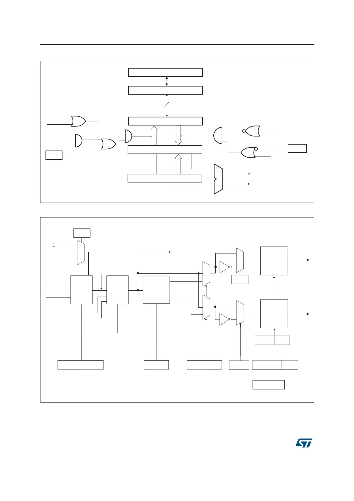
Figure 297. Capture/compare channel 1 main circuit
Figure 298. Output stage of capture/compare channel (channel 1, idem ch. 2, 3 and 4)
1. tim_ocxref, where x is the rank of the complementary channel
MSv63030V1
CC1E
compare shadow register
Comparator
Capture/compare preload register
Counter
IC1PS
CC1S[0]
CC1S[1]
Capture
Input mode
CC1S[0]
CC1S[1]
Output mode
UEV
OC1PE
(from time
base unit)
Compare
transfer
APB Bus
16/32-bit
MCU-peripheral interface
TIMx_CCMR1
OC1PE
CNT>CCR1
CNT=CCR1
TIMx_EGR
CC1G
MSv62323V3
Output
mode
controller
Ouput
selector
CNT>CCR1
CNT=CCR1
TIMx_CCMR1
OC1M[3:0]
tim_oc1ref
OC1CE
Dead-time
generator
tim_oc1_dt
tim_oc1n_dt
DTG[7:0]
TIMx_BDTR
‘0’
‘0’
CC1E
TIMx_CCER
CC1NE
0
1
CC1P
TIMx_CCER
0
1
CC1NP
TIMx_CCER
tim_oc1
Output
enable
circuit
tim_oc1n
CC1E
TIMx_CCER
CC1NE
OSSI
TIMx_BDTR
MOE OSSR
0x
10
11
11
01
x0
tim_ocxref
(1)
tim_oc1refc
To the master mode
controller
Output
enable
circuit
0
1
tim_oc5ref
ocref_clr_int
tim_ocref_clr
tim_etrf
OCCS
TIMx_SMCR
OIS1N
TIMx_CR2
OIS1
 Loading...


