Flexible static memory controller (FSMC) RM0440
518/2126 RM0440 Rev 4
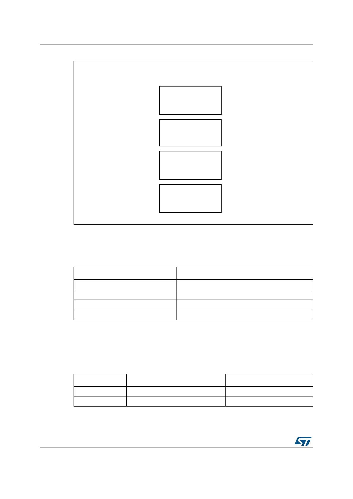
Figure 53. FMC memory banks
19.5.1 NOR/PSRAM address mapping
HADDR[27:26] bits are used to select one of the four memory banks as shown in Table 119.
The HADDR[25:0] bits contain the external memory address. Since HADDR is a byte
address whereas the memory is addressed at word level, the address actually issued to the
memory varies according to the memory data width, as shown in the following table.
MSv34475V2
Bank 1
4 x 64 Mbyte
NOR/PSRAM/SRAM
Supported memory type
Bank
0x6000 0000
Address
0x6FFF FFFF
0x7000 0000
0x7FFF FFFF
0x8000 0000
0x8FFF FFFF
0x9000 0000
0x9FFF FFFF
Not used
Bank 3
4 x 64 Mbyte
Not used
NAND Flash memory
Table 119. NOR/PSRAM bank selection
HADDR[27:26]
(1)
1. HADDR are internal AHB address lines that are translated to external memory.
Selected bank
00 Bank 1 - NOR/PSRAM 1
01 Bank 1 - NOR/PSRAM 2
10 Bank 1 - NOR/PSRAM 3
11 Bank 1 - NOR/PSRAM 4
Table 120. NOR/PSRAM External memory address
Memory width
(1)
1. In case of a 16-bit external memory width, the FMC internally uses HADDR[25:1] to generate the address
for external memory FMC_A[24:0].
Whatever the external memory width, FMC_A[0] should be connected to external memory address A[0].
Data address issued to the memory Maximum memory capacity (bits)
8-bit HADDR[25:0] 64 Mbytes x 8 = 512 Mbit
16-bit HADDR[25:1] >> 1 64 Mbytes/2 x 16 = 512 Mbit
 Loading...


