General-purpose timers (TIM2/TIM3/TIM4/TIM5) RM0440
1302/2126 RM0440 Rev 4
1. Configure TIM_mstr master mode to send its Enable as trigger output (MMS=001 in the
TIM_mstr_CR2 register).
2. Configure TIM_mstr slave mode to get the input trigger from tim_ti1 (TS=00100 in the
TIM_mstr_SMCR register).
3. Configure TIM_mstr in trigger mode (SMS=110 in the TIM_mstr_SMCR register).
4. Configure the TIM_mstr in Master/Slave mode by writing MSM=1 (TIM_mstr_SMCR
register).
5. Configure TIM_slv to get the input trigger from TIM_mstr (TS=00000 in the
TIM_slv_SMCR register).
6. Configure TIM_slv in trigger mode (SMS=110 in the TIM_slv_SMCR register).
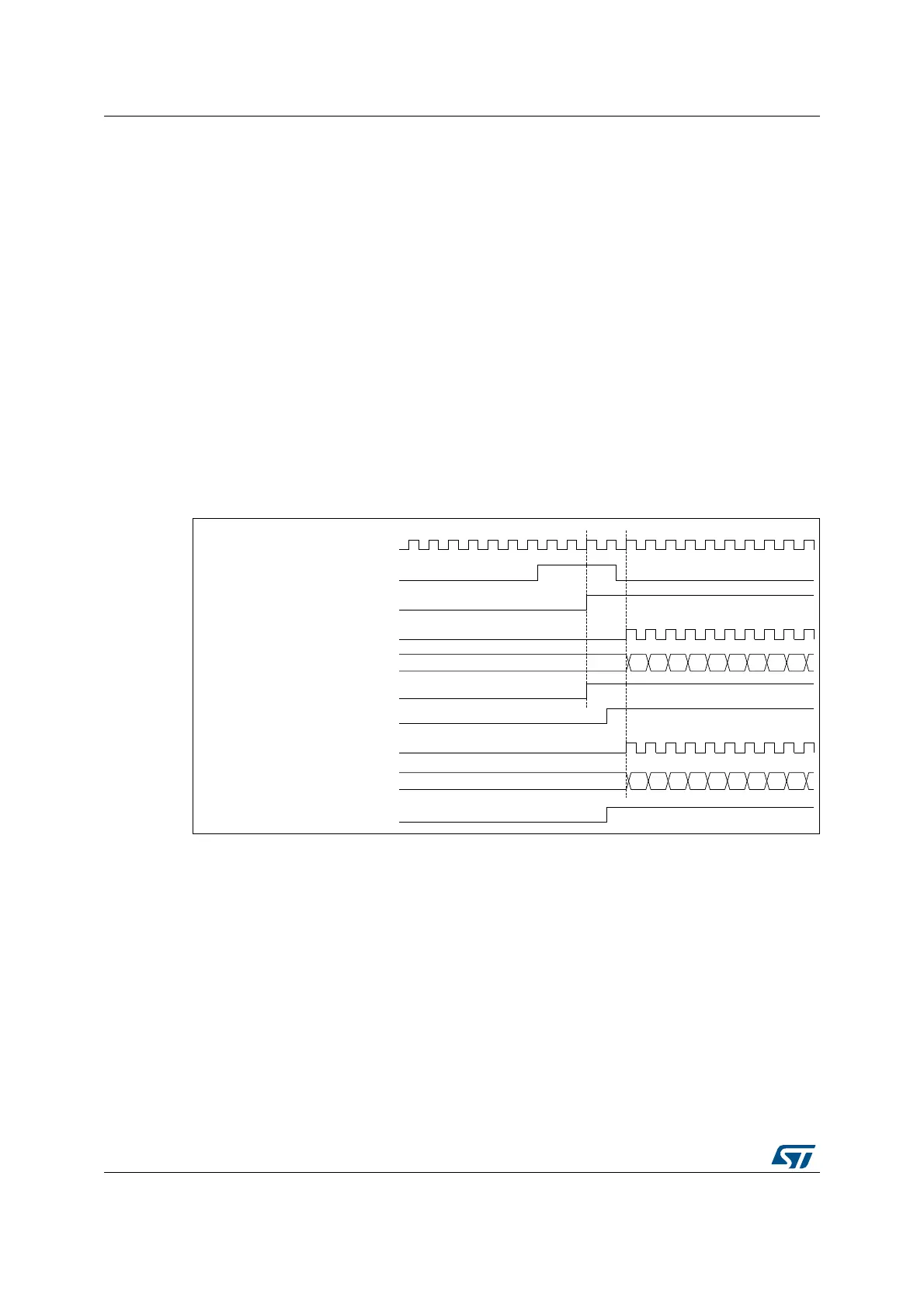
When a rising edge occurs on tim_ti1 (TIM_mstr), both counters starts counting
synchronously on the internal clock and both TIF flags are set.
Note: In this example both timers are initialized before starting (by setting their respective UG
bits). Both counters starts from 0, but an offset can easily be inserted between them by
writing any of the counter registers (TIMx_CNT). One can see that the master/slave mode
insert a delay between CNT_EN and CK_PSC on TIM_mstr.
Figure 438. Triggering TIM_mstr and TIM_slv with TIM_mstr tim_ti1 input
Note: The clock of the slave peripherals (timer, ADC, ...) receiving the tim_trgo signal must be
enabled prior to receive events from the master timer, and the clock frequency (prescaler)
must not be changed on-the-fly while triggers are received from the master timer.
29.4.24 DMA burst mode
The TIMx timers have the capability to generate multiple DMA requests upon a single event.
The main purpose is to be able to re-program part of the timer multiple times without
software overhead, but it can also be used to read several registers in a row, at regular
intervals.
The DMA controller destination is unique and must point to the virtual register TIMx_DMAR.
On a given timer event, the timer launches a sequence of DMA requests (burst). Each write
into the TIMx_DMAR register is actually redirected to one of the timer registers.
MSv62380V1
tim_ker_ck
tim_slv_CNT
TIM_mst counter enable (CEN bit))
tim_slv TIF bit
01
tim_mstr_CNT
02 03 04 05 06 07 08 0900
01 02 03 04 05 06 07 08 0900
TIM_slv counter enable (CEN bit)
tim_mstr TIF bit
tim_mstr_psc_ck
tim_mstr_ti1
tim_slv_psc_ck
 Loading...


