RM0440 Rev 4 141/2126
RM0440 Embedded Flash memory (FLASH) for category 3 devices
228
3.7.13 Flash PCROP2 Start address register (FLASH_PCROP2SR)
Address offset: 0x44
Reset value: 0xFFFF XXXX
Access: no wait state when no Flash memory operation is on going, word access.
3.7.14 Flash PCROP2 End address register (FLASH_PCROP2ER)
Address offset: 0x48
Reset value: 0x0000 XXXX
Access: no wait state when no Flash memory operation is on going, word access
Bits 31:23 Reserved, must be kept cleared
Bits 22:16 WRP1B_END: WRP second area “B” end offset
DBANK=1
WRP1B_END contains the last page of the WRP second area for bank1.
DBANK=0
WRP1B_END contains the last page of the WPR second area for all memory.
Bits 15:7 Reserved, must be kept cleared
Bits 6:0 WRP1B_STRT: WRP second area “B” start offset
DBANK=1
WRP1B_STRT contains the last page of the WRP second area for bank1.
DBANK=0
WRP1B_STRT contains the last page of the WPR second area for all memory.
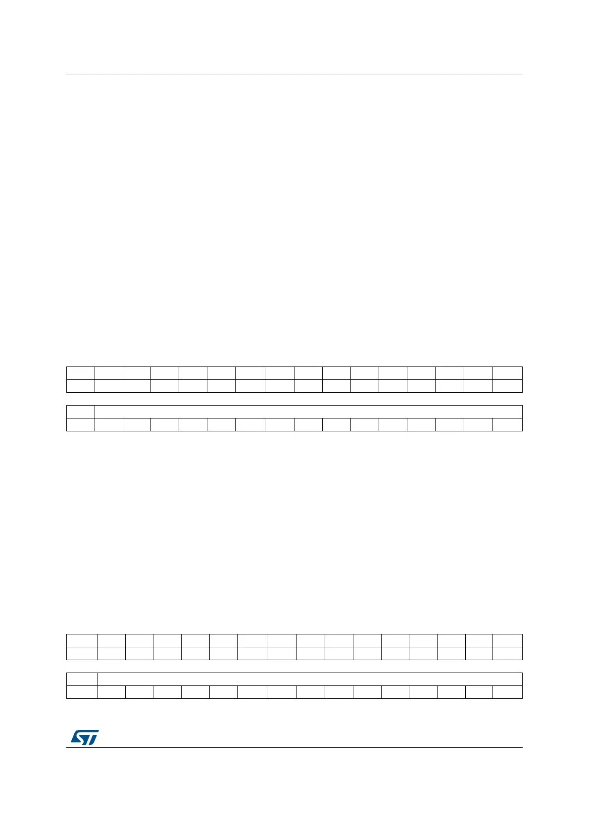
31 30 29 28 27 26 25 24 23 22 21 20 19 18 17 16
Res. Res. Res. Res. Res. Res. Res. Res. Res. Res. Res. Res. Res. Res. Res. Res.
1514131211109 8 765432 1 0
Res. PCROP2_STRT[14:0]
rw rw rw rw rw rw rw rw rw rw rw rw rw rw rw
Bits 31:15 Reserved, must be kept cleared
Bits 14:0 PCROP2_STRT: PCROP area start offset
DBANK=1
PCROP2_STRT contains the first double-word of the PCROP area for bank 2.
DBANK=0
PCROP2_STRT contains the first double-word PCROP area for all memory.
31 30 29 28 27 26 25 24 23 22 21 20 19 18 17 16
Res. Res. Res. Res. Res. Res. Res. Res. Res. Res. Res. Res. Res. Res. Res. Res.
15 14 13 12 11 10 9 8 7 6 5 4 3 2 1 0
Res. PCROP2_END[14:0]
rw rw rw rw rw rw rw rw rw rw rw rw rw rw rw
 Loading...


