RM0440 Rev 4 357/2126
RM0440 General-purpose I/Os (GPIO)
368
Figure 28. Output configuration
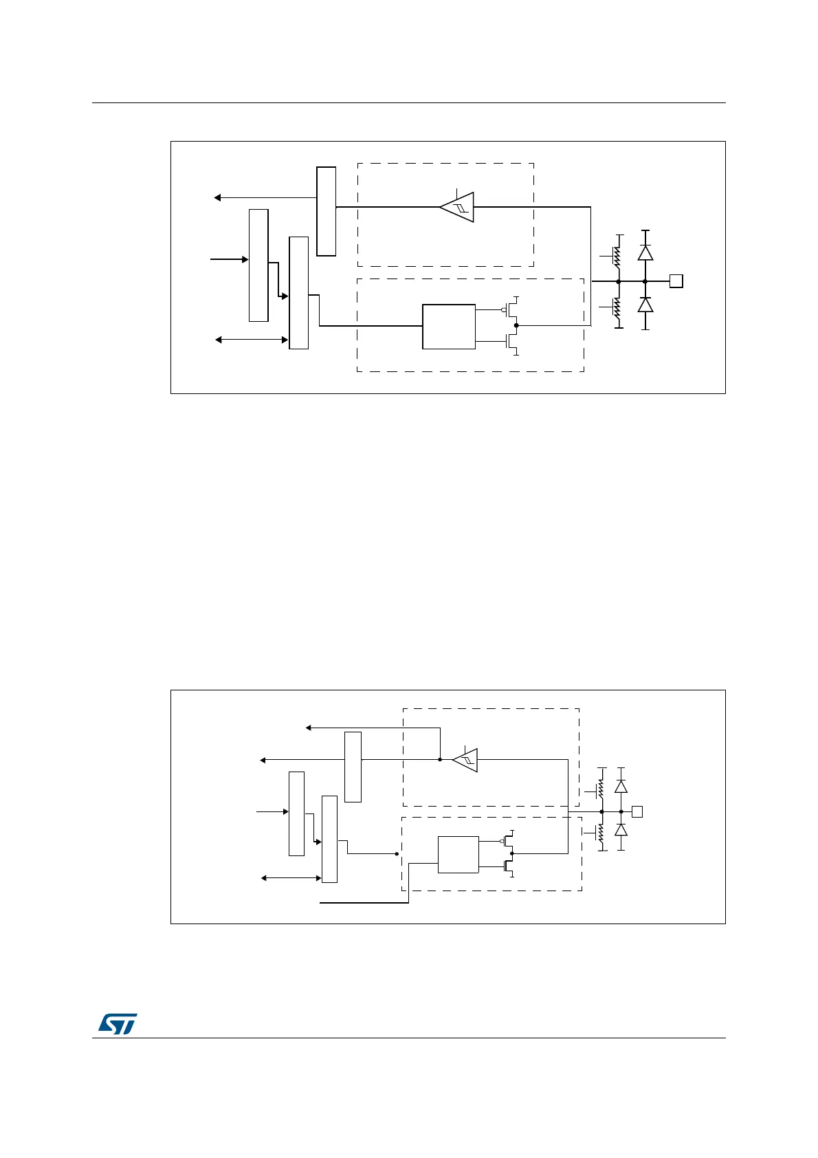
9.3.11 Alternate function configuration
When the I/O port is programmed as alternate function:
• The output buffer can be configured in open-drain or push-pull mode
• The output buffer is driven by the signals coming from the peripheral (transmitter
enable and data)
• The Schmitt trigger input is activated
• The weak pull-up and pull-down resistors are activated or not depending on the value
in the GPIOx_PUPDR register
• The data present on the I/O pin are sampled into the input data register every AHB
clock cycle
• A read access to the input data register gets the I/O state
Figure 29 shows the Alternate function configuration of the I/O port bit.
Figure 29. Alternate function configuration
Push-pull or
Open-drain
Output
control
V
DDIOx
V
SS
TTL Schmitt
trigger
on
Input driver
Output driver
P-MOS
N-MOS
Input data register
Output data register
Read/write
Read
Bit set/reset registers
Write
on/off
pull
pull
on/off
V
DDIOx
V
SS
V
SS
V
DDIOx
protection
diode
protection
diode
down
up
I/O pin
MS31478V1
MSv34756V1
Alternate function output
Alternate function input
push-pull or
open-drain
From on-chip
peripheral
To on-chip
peripheral
Output
control
V
DD
V
SS
TTL Schmitt
trigger
on
Input driver
Output driver
P-MOS
N-MOS
Input data register
Output data register
Read/write
Read
Bit set/reset registers
Write
on/off
on/off
VDDIOx
V
SS
V
SS
protection
diode
protection
diode
Pull
Pull
I/O pin
down
up
VDDIOx
 Loading...


