RM0440 Rev 4 1389/2126
RM0440 General-purpose timers (TIM15/TIM16/TIM17)
1445
1. Configure the corresponding DMA channel as follows:
– DMA channel peripheral address is the DMAR register address
– DMA channel memory address is the address of the buffer in the RAM containing
the data to be transferred by DMA into the CCRx registers.
– Number of data to transfer = 3 (See note below).
– Circular mode disabled.
2. Configure the DCR register by configuring the DBA and DBL bit fields as follows:
DBL = 3 transfers, DBA = 0xE.
3. Enable the TIMx update DMA request (set the UDE bit in the DIER register).
4. Enable TIMx
5. Enable the DMA channel
This example is for the case where every CCRx register is to be updated once. If every
CCRx register is to be updated twice for example, the number of data to transfer should be
6. Let's take the example of a buffer in the RAM containing data1, data2, data3, data4, data5
and data6. The data is transferred to the CCRx registers as follows: on the first update DMA
request, data1 is transferred to CCR2, data2 is transferred to CCR3, data3 is transferred to
CCR4 and on the second update DMA request, data4 is transferred to CCR2, data5 is
transferred to CCR3 and data6 is transferred to CCR4.
Note: A null value can be written to the reserved registers.
30.4.28 TIM15/TIM16/TIM17 DMA requests
The TIM15/TIM16/TIM17 can generate a DMA requests, as shown in Table 296.
30.4.29 Debug mode
When the microcontroller enters debug mode (Cortex
®
-M4 with FPU core halted), the TIMx
counter can either continue to work normally or stop.
The behavior in debug mode can be programmed with a dedicated configuration bit per
timer in the Debug support (DBG) module.
For safety purposes, when the counter is stopped, the outputs are disabled (as if the MOE
bit was reset). The outputs can either be forced to an inactive state (OSSI bit = 1), or have
their control taken over by the GPIO controller (OSSI bit = 0) to force them to Hi-Z.
For more details, refer to the debug section.
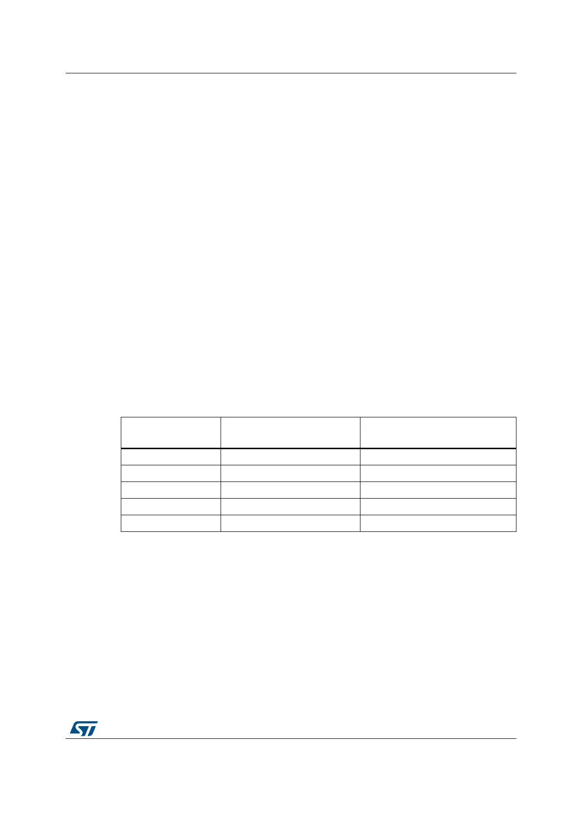
Table 296. DMA request
DMA acronym DMA request
Enable
control bit
TIM_UP Update UDE
TIM_CH1 Capture/compare 1 CC1DE
TIM_CH2
(1)
1. Available for TIM15 only.
Capture/compare 2 CC2DE
TIM_COM Commutation (COM) COMDE
TIM_TRIG
(1)
Trigger TDE
 Loading...


