Flexible static memory controller (FSMC) RM0440
542/2126 RM0440 Rev 4
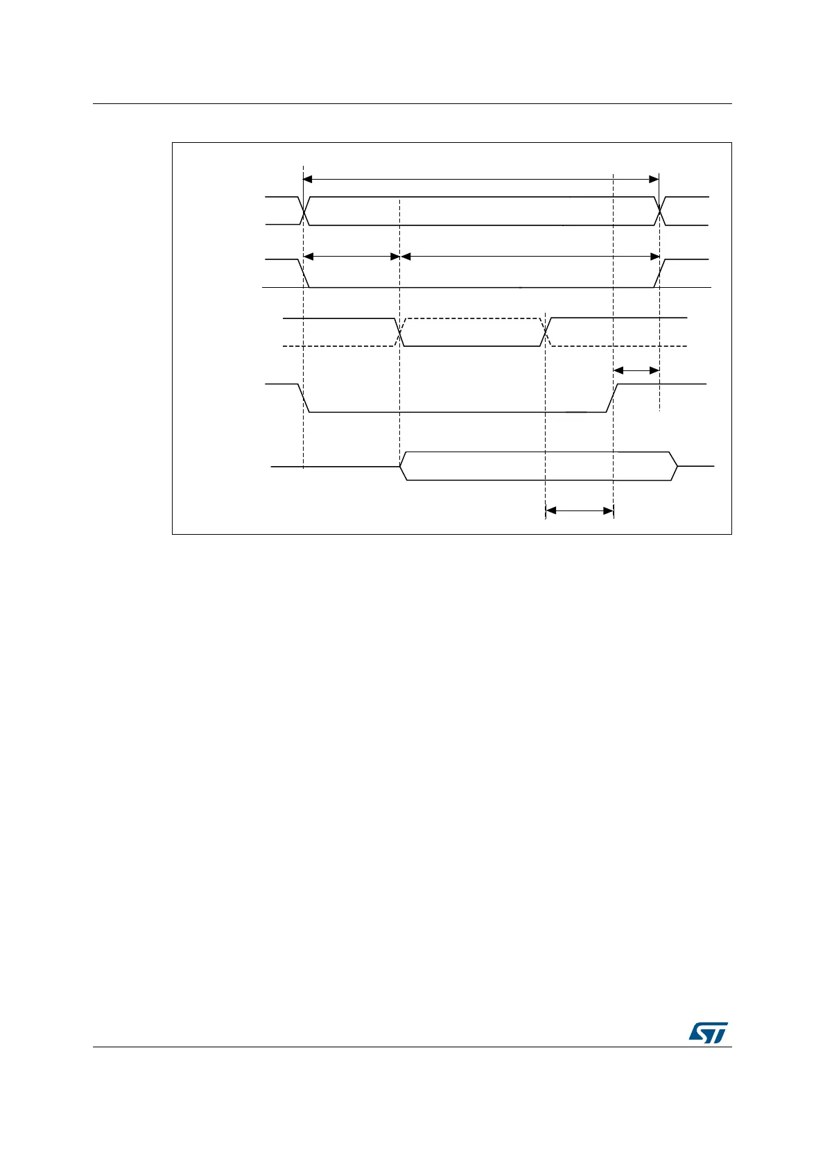
Figure 68. Asynchronous wait during a write access waveforms
1. NWAIT polarity depends on WAITPOL bit setting in FMC_BCRx register.
CellularRAM™ (PSRAM) refresh management
The CellularRAM™ does not allow maintaining the chip select signal (NE) low for longer
than the t
CEM
timing specified for the memory device. This timing can be programmed in the
FMC_PCSCNTR register. It defines the maximum duration of the NE low pulse in HCLK
cycles for asynchronous accesses and FMC_CLK cycles for synchronous accesses
19.6.5 Synchronous transactions
The memory clock, FMC_CLK, is a submultiple of HCLK. It depends on the value of
CLKDIV and the MWID/ AHB data size, following the formula given below:
Whatever MWID size: 16 or 8-bit, the FMC_CLK divider ratio is always defined by the
programmed CLKDIV value.
Example:
• If CLKDIV=1, MWID = 16 bits, AHB data size=8 bits, FMC_CLK=HCLK/2.
NOR Flash memories specify a minimum time from NADV assertion to CLK high. To meet
this constraint, the FMC does not issue the clock to the memory during the first internal
clock cycle of the synchronous access (before NADV assertion). This guarantees that the
rising edge of the memory clock occurs in the middle of the NADV low pulse.
Data latency versus NOR memory latency
The data latency is the number of cycles to wait before sampling the data. The DATLAT
value must be consistent with the latency value specified in the NOR Flash configuration
MSv40168V1
A[25:0]
NWE
Memory transaction
D[15:0]
NEx
data driven by FMC
3HCLK
address phase
data setup phase
1HCLK
NWAIT
don’t care don’t care
 Loading...


