RM0440 Rev 4 831/2126
RM0440 True random number generator (RNG)
843
26.3 RNG functional description
26.3.1 RNG block diagram
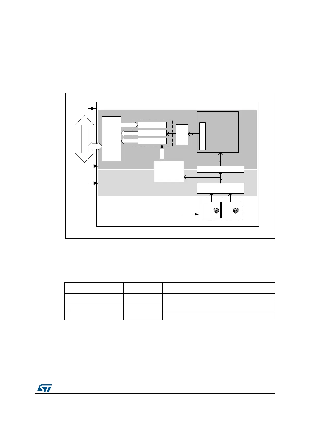
Figure 179 shows the RNG block diagram.
Figure 179. RNG block diagram
26.3.2 RNG internal signals
Table 204 describes a list of useful-to-know internal signals available at the RNG level, not
at the STM32 product level (on pads).
MSv42097V2
True RNG
RNG_CR
RNG_SR
AHB
interface
control
status
RNG_DR
data
Analog
noise
source 1
Banked Registers
Sampling &
Normalization (x 2)
Analog noise source
Fault detection
Clock checker
2-bit
Alarms
Analog
noise
source 2
4x32-bit
FIFO
Conditioning logic
32-bit
128-bit data output
en_osc
32-bit AHB Bus
rng_it
rng_clk
AHB clock domain
RNG clock domain
Raw data shift reg
128-bit
Table 204. RNG internal input/output signals
Signal name Signal type Description
rng_it Digital output RNG global interrupt request
rng_hclk Digital input AHB clock
rng_clk Digital input RNG dedicated clock, asynchronous to rng_hclk
 Loading...


