RM0440 Rev 4 669/2126
RM0440 Analog-to-digital converters (ADC)
724
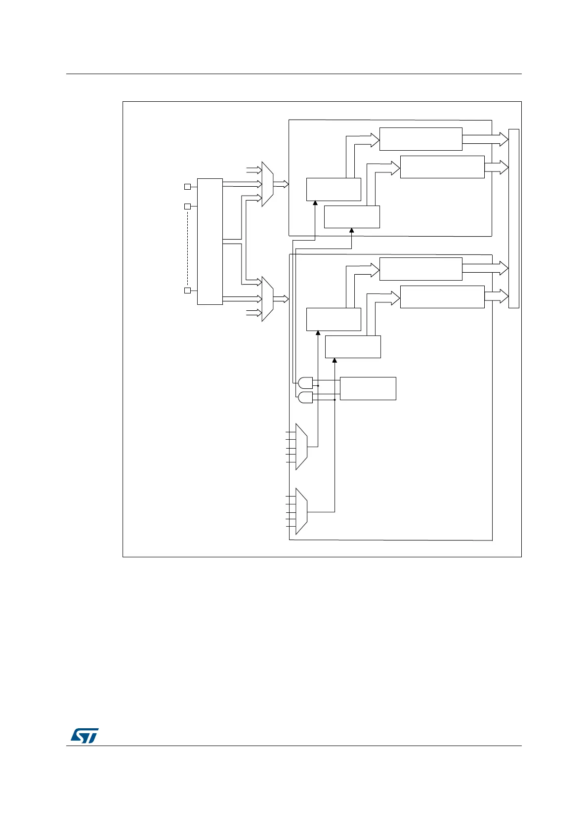
Figure 137. Dual ADC block diagram
(1)
1. External triggers also exist on slave ADC but are not shown for the purposes of this diagram.
2. The ADC common data register (ADCx_CDR) contains both the master and slave ADC regular converted data.
MSv36025V2
Regular data register (16-
bits)
Injected data registers (4
x16-bits)
Injected
channels
Regular
channels
Regular data register (16-
bits)
Injected data registers (4
x16-bits)
Injected
channels
Regular
channels
Address/data bus
ADCx_INN2
ADCx_INP2
Dual mode
control
Master ADC
Slave ADC
Start trigger mux.
(regular group)
Start trigger mux.
(injected group)
Internal analog inputs
Internal triggers
Internal analog inputs
ADCx_INN1
ADCx_INP1
ADCx_INN16
ADCx_INP16
 Loading...


