Advanced-control timers (TIM1/TIM8/TIM20) RM0440
1136/2126 RM0440 Rev 4
The tim_brk has a higher priority than tim_brk2 input, as described in Table 258.
Note: tim_brk2 must only be used with OSSR = OSSI = 1.
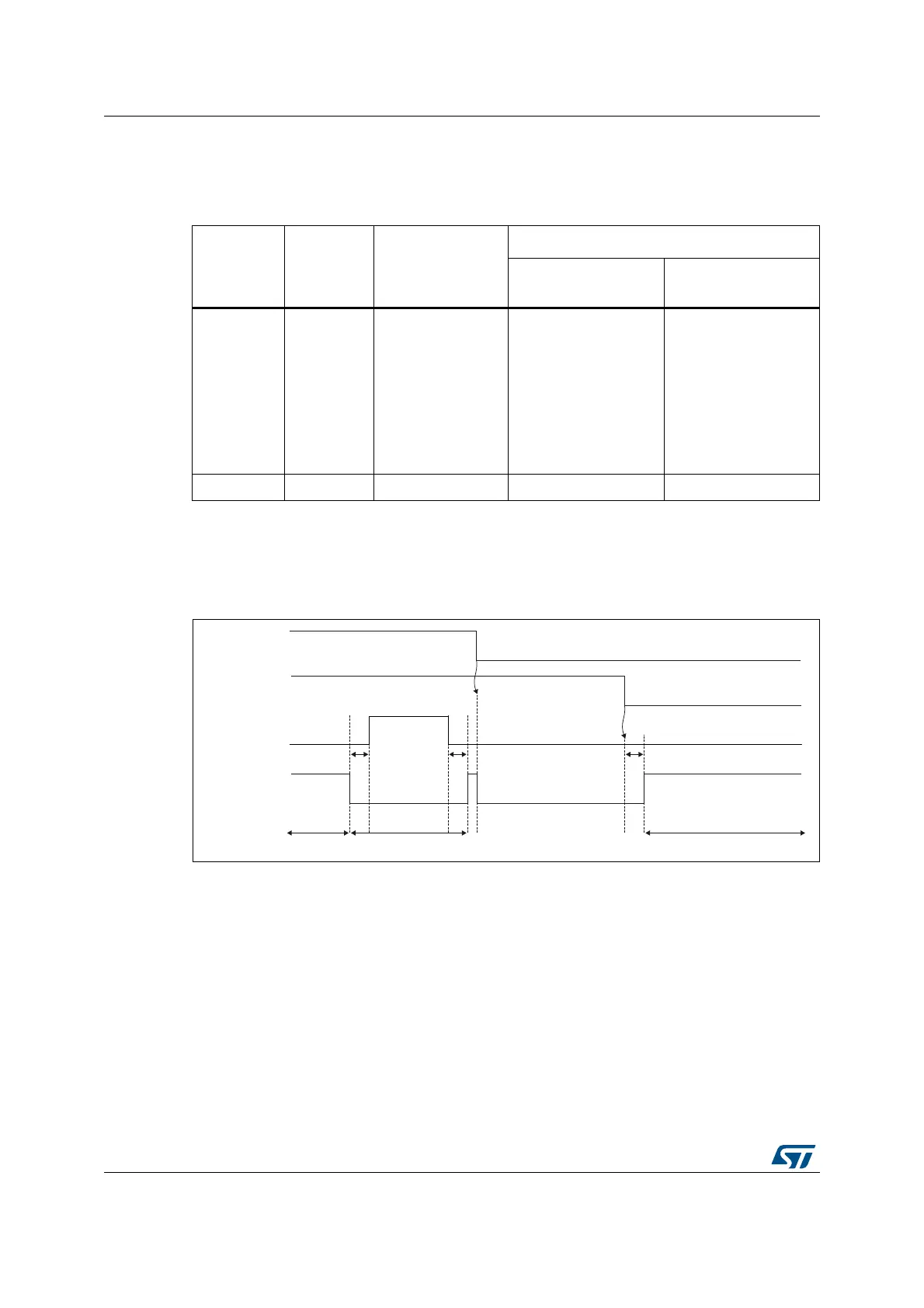
Figure 318 gives an example of tim_ocx and tim_ocxn output behavior in case of active
signals on tim_brk and tim_brk2 inputs. In this case, both outputs have active high polarities
(CCxP = CCxNP = 0 in TIMx_CCER register).
Figure 318. PWM output state following tim_brk and tim_brk2 assertion (OSSI=1)
Table 258. Behavior of timer outputs versus tim_brk/tim_brk2 inputs
tim_brk tim_brk2
Timer outputs
state
Typical use case
tim_ocxn output
(low side switches)
tim_ocx output
(high side switches)
Active X
– Inactive then
forced output
state (after a
deadtime)
– Outputs disabled
if OSSI = 0
(control taken
over by GPIO
logic)
ON after deadtime
insertion
OFF
Inactive Active Inactive OFF OFF
MSv62338V1
tim_brk2
tim_brk
tim_ocx
I/O state
Deadtime Deadtime
Active Inactive Idle
tim_ocxn
 Loading...


