Embedded Flash memory (FLASH) for category 3 devices RM0440
140/2126 RM0440 Rev 4
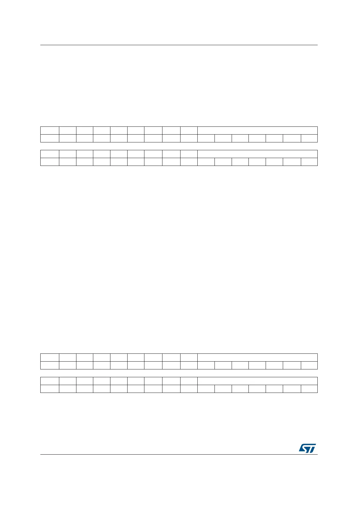
3.7.11 Flash Bank 1 WRP area A address register (FLASH_WRP1AR)
Address offset: 0x2C
Reset value: 0x00XX 00XX. Register bits are loaded with values from Flash memory at
OBL.
Access: no wait state when no Flash memory operation is on going, word, half-word and
byte access
3.7.12 Flash Bank 1 WRP area B address register (FLASH_WRP1BR)
Address offset: 0x30
Reset value: 0x00XX 00XX. Register bits are loaded with values from Flash memory at
OBL.
Access: no wait state when no Flash memory operation is on going, word, half-word and
byte access
31 30 29 28 27 26 25 24 23 22 21 20 19 18 17 16
Res. Res. Res. Res. Res. Res. Res. Res. Res. WRP1A_END[6:0]
rw rw rw rw rw rw rw
15 14 13 12 11 10 9 8 7 6 5 4 3 2 1 0
Res. Res. Res. Res. Res. Res. Res. Res. Res. WRP1A_STRT[6:0]
rw rw rw rw rw rw rw
Bits 31:23 Reserved, must be kept cleared
Bits 22:16 WRP1A_END: WRP first area “A” end offset
DBANK=1
WRP1A_END contains the last page of WRP first area in bank1.
DBANK=0
WRP1A_END contains the last page of WRP first area for all memory.
Bits 15:7 Reserved, must be kept cleared
Bits 6:0 WRP1A_STRT: WRP first area “A” start offset
DBANK=1
WRP1A_STRT contains the first page of WRP first area for bank1.
DBANK=0
WRP1A_STRT contains the first page of WRP first area for all memory.
31 30 29 28 27 26 25 24 23 22 21 20 19 18 17 16
Res. Res. Res. Res. Res. Res. Res. Res. Res. WRP1B_END[6:0]
rw rw rw rw rw rw rw
15 14 13 12 11 10 9 8 7 6 5 4 3 2 1 0
Res. Res. Res. Res. Res. Res. Res. Res. Res. WRP1B_STRT[6:0]
rw rw rw rw rw rw rw
 Loading...


