RM0440 Rev 4 85/2126
RM0440
91
2.3 Bit banding
The Cortex
®
-M4 with FPU memory map includes two bit-band regions. These regions map
each word in an alias region of memory to a bit in a bit-band region of memory. Writing to a
word in the alias region has the same effect as a read-modify-write operation on the
targeted bit in the bit-band region.
In the STM32G4 Series devices both the peripheral registers and the SRAM are mapped to
a bit-band region, so that single bit-band write and read operations are allowed. The
operations are only available for Cortex
®
-M4 with FPU accesses, and not from other bus
masters (e.g. DMA).
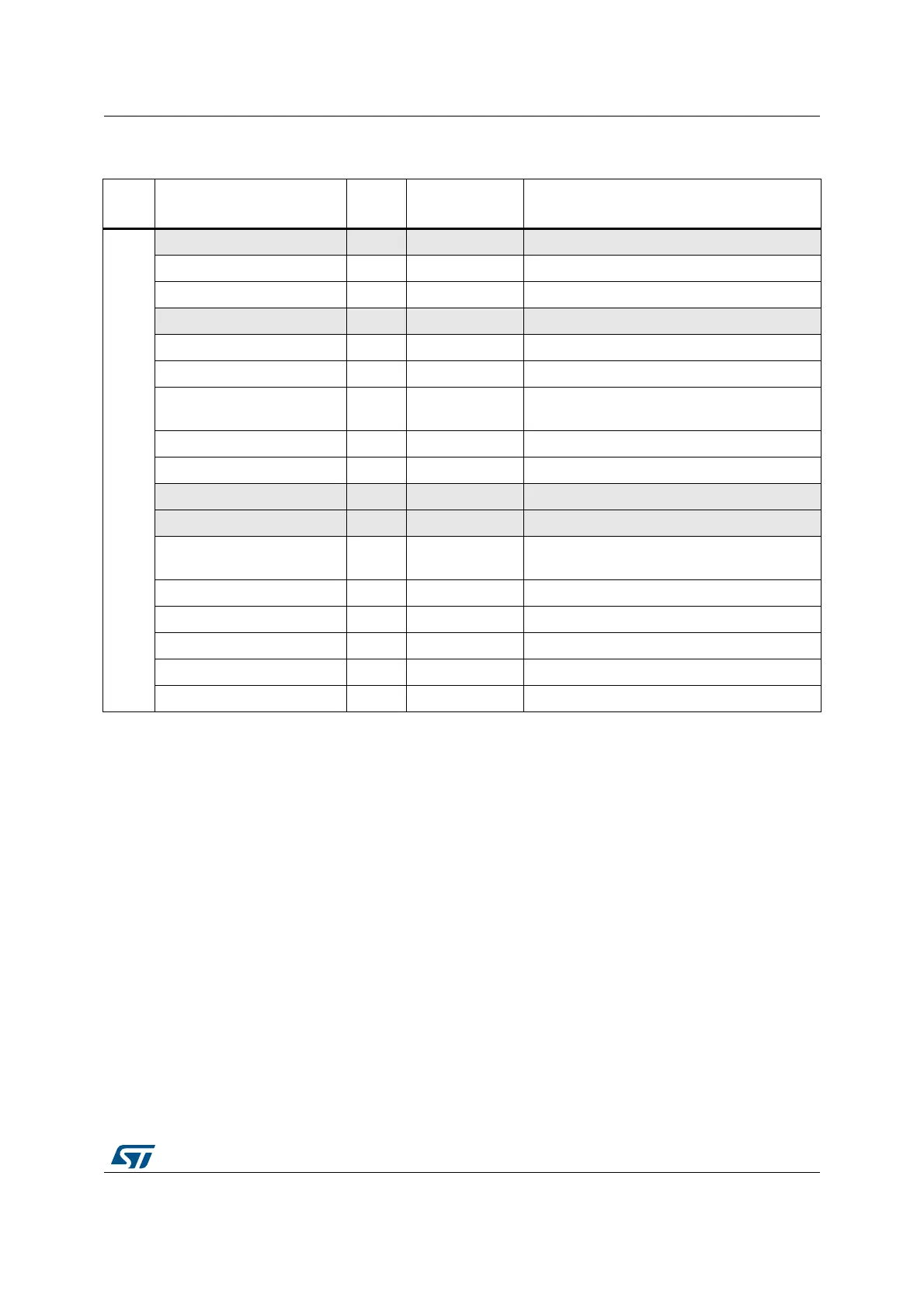
APB1
Cont.
0x4000 4000 - 0x4000 43FF 1KB Reserved -
0x4000 3C00 - 0x4000 3FFF 1 KB SPI3/I2S3 Section 39.9.10: SPI/I2S register map
0x4000 3800 - 0x4000 3BFF 1 KB SPI2/I2S2 Section 39.9.10: SPI/I2S register map
0x4000 3400 - 0x4000 37FF 1KB Reserved -
0x4000 3000 - 0x4000 33FF 1 KB IWDG Section 42.4.6: IWDG register map
0x4000 2C00 - 0x4000 2FFF 1 KB WWDG Section 43.5.4: WWDG register map
0x4000 2800 - 0x4000 2BFF 1 KB
RTC & BKP
Registers
Section 35.6.21: RTC register map
0x4000 2400 - 0x4000 27FF 1 KB TAMP Section 36.6.9: TAMP register map
0x4000 2000 - 0x4000 23FF 1 KB CRS Section 8.7.5: CRS register map
0x4000 1C00 - 0x4000 1FFF 1KB Reserved -
0x4000 1800 - 0x4000 1BFF 1KB Reserved -
0x4000 1400 - 0x4000 17FF 1 KB TIM7
Section 29.5.31: TIMx register
mapSection 31.4.9: TIMx register map
0x4000 1000 - 0x4000 13FF 1 KB TIM6 Section 31.4.9: TIMx register map
0x4000 0C00 - 0x4000 0FFF 1 KB TIM5 Section 29.5.31: TIMx register map
0x4000 0800 - 0x4000 0BFF 1 KB TIM4 Section 29.5.31: TIMx register map
0x4000 0400 - 0x4000 07FF 1 KB TIM3 Section 29.5.31: TIMx register map
0x4000 0000 - 0x4000 03FF 1 KB TIM2 Section 29.5.31: TIMx register map
1. Refer to Table 1: STM32G4 Series memory density, Table 2: Product specific features and to the device datasheets for the
GPIO ports and peripherals available on your device. the memory area corresponding to unavailable GPIO ports or
peripherals are reserved (highlighted in gray).
Table 3. STM32G4 Series memory map and peripheral register boundary
addresses
(1)
(continued)
Bus Boundary address
Size
(bytes)
Peripheral Peripheral register map
 Loading...


